Core memory as wall art. This is a Burroughs 3-wire planar array comprising 32,768 words of 20 bits/word.
|
|
Core memory as wall art. This is a Burroughs 3-wire planar array comprising 32,768 words of 20 bits/word.
|
If you have looked at a core memory plane, or a picture of one (or need to repair one in the absence of service info), and wondered just why the cores and wires were arranged in such patterns, this article may provide some answers. For those old enough to have direct professional experience with core-based systems the following may be 'old hat', for those too young it may fill in some gaps in the common literature.
This article is based primarily on the examination of several core memory modules, along with some written references. It covers the basic principles, functional electrical arrangement and physical topologies of the predominant forms of core memory systems: the 3-dimensional 4-wire and 3-D 3-wire systems. It does not claim to be a comprehensive review of the technology as there were other techniques and organisations used in addition to those described here.
Contents |
|
Core memory was developed in the late-1940s/early-1950s as part of the Whirlwind computer project at MIT. Whirlwind had started out during WWII as a 'configurable' hydraulic-servo-based aircraft simulator and migrated over the years into a digital electronic real-time processing system. It eventually found it's raison-d'etre as a proof-of-concept for what would become the SAGE continent-wide nuclear-attack bomber-detection system.
Whirlwind became very expensive as it progressed and it's justification for existence in the face of all the other U.S. federally-funded computer projects - it's distinguishing characteristic - was it's real-time processing capabilities. It had a relatively small word size for the day (16 bits) and a hardware multiplier to help meet the real-time objectives, and it likewise needed a fast read/write memory. Unfortunately, the holding-beam form of storage-tube memory the developers of Whirlwind had produced for the machine was proving to be unreliable and required frequent maintenance.
In 1949 Jay Forrester, the director of the Whirlwind project, set about to find a better form of memory. The long average access times of the other popular memory systems of the day - acoustic delay lines and magnetic drums - made them inadequate for Whirlwind. Recent developments in ferro-magnetic materials caught his attention and he quietly began to explore their potential as a two-state memory. A small core-memory test system was constructed and was successful in showing core's viability. In 1953 the storage-tube memory was discarded and Whirlwind was converted to using core memory.
Core quickly became the predominant form of main memory for computers. Other machines, such as the IBM 701 and the NORC (Naval Ordnance Research Calculator), also had their storage-tube memory replaced with core. Core memory rode through the transitions of logic technology from vacuum tubes to transistors to SSI ICs and weathered competition from thin-film and plated-wire memory technologies in the 1960s. It was finally replaced by semiconductor LSI technology during the mid-to-late-1970s.
Core continued to see use for many years in some special-requirements systems, where use over time helped prove design reliability and where the non-volatility of core might be used to advantage, such as for speedy recovery of state in real-time systems.
I have seen it in service as recently as 2004 in a telephony control application, the design and construction of which dates from the late-1970s/early-1980s, and it still functions in a few old systems maintained by computer museums and collectors.
It's legacy lives on in the so-named "core" files produced on UNIX systems when a program crashes.

|
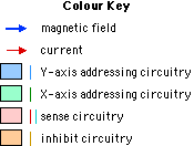
The hysteresis-loop graph in figure 2a describes the response of the magnetic field of the core to the current in the wire through the core.
As a memory device the benefit of hysteresis is the bistable characteristic, significantly reducing noise sensitivity of the device and eliminating state decay and the consequent need for refreshing.
The points
|
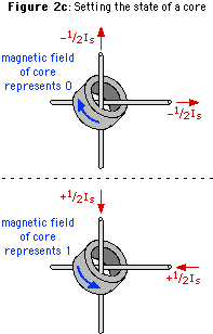
To read the 'memory', the core will be forced into a given state (figure 2d). If the core was in the opposite state, the reversal of the core's magnetic field constitutes a changing magnetic field which will induce a detectable current pulse in a third wire threaded through the core (referred to as the sense wire). If the core was already in the given state, while there is some perturbation of it's magnetic field by the addressing currents, this perturbation and the current induced by it are smaller and distinguishable from those of a field reversal. Sensing issues are dealt with further in the Sensing section.
|
|
|
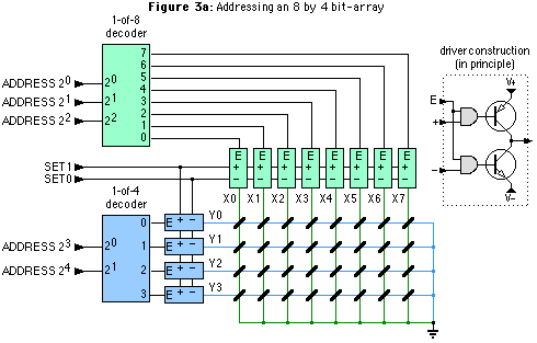
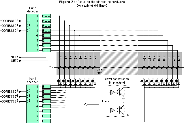
This construct can be found in use for arrays of small dimensions but for larger arrays it is common to make the address decoders simpler and reduce the number of drivers by taking advantage of the ability to control both ends of an address wire.
When considering one axis of n address wires, rather than using a
For example, figure 3b shows one 64-wire axis reduced to two
In practice, a wide variety of decoder/driver designs were produced and aspects of real implementations may differ from those presented here in terms of control signal organisation, power supply configuration, etc. Of particular note, pulse transformers were widely used in the decoder/drivers.
|
Note the preceding diagrams show the functional electrical organisation of addressing a bit-array, the actual physical organisation adds some twists (literally) and is discussed in the following section.
|
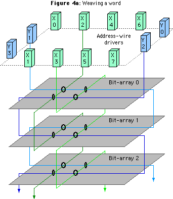
It is not difficult to see this produces a problem: setting the state of one bit sets all the bits of that word to the same state. The usual remedy for this is to run another wire through the cores, referred to as the inhibit wire. Each bit-array will have it's own inhibit wire and driver (figure 4b).
When writing a word, if a bit of that word is not to be altered the according inhibit wire will carry a current opposed to that of the parallel address wire, thus inhibiting the address wire's influence by reducing the sum current through the addressed core to below the saturation level.
Alternating address wires are fed from opposite directions, which matches the back-and-forth weave of the inhibit wire. The orientation of half the cores is rotated 90 degrees so they still catch the current-direction combinations which sum to produce the saturation level.
The sequences involved in writing are discussed further in the Read/Write Cycles and Interfacing section.
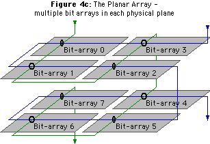
Figure 4a also gives a graphic indication of the source of the term 'core stack'.
In practice, while there were early implementations that followed this structure physically,
later implementations generally reduced the stack height by placing multiple bit-arrays in the same physical plane (figure 4c), referred to as a planar array.
|
|
While searching for a problem in an 8 KWord core memory module for an HP2116C computer I was perplexed when I could find only enough address drivers to address 4 KWords. How was it that another 4K was being addressed?
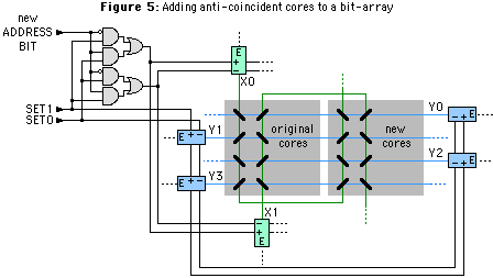
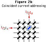
Notice that with 2 address wires going through each core and 2 possible directions of current through each wire there are 4 possible combinations of current through each core. However, only 2 combinations are used: the 2 which go through the core from the same side (are coincident) and so sum to produce the saturation level. In the other 2 combinations (anti-coincident) the address wire currents cancel each other and have no effect on the core.
If another set of cores is added to a bit-array in such a manner that one axis of address wires goes through the new cores from the other direction (the X-axis in figure 5), then this new set will respond to the other 2 current combinations while ignoring the original 2 combinations, and vice-versa for the original set. The combinations are shown in table 5, where "+" and "-" indicate the direction of address-wire currents from the drivers.
|
|
|||||||||||||||||||||||||||||||
To address the new cores the current direction on the redirected axis of address wires must be reversed. The drivers are already capable of sending current in either direction, so all that is required is to add a few logic gates to swap the influence of the SET1 and SET0 signals on the one axis of address-wire drivers. If the "new ADDRESS BIT" signal is 0 the original cores will be addressed; if 1, the new cores are addressed.
|
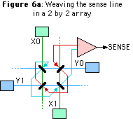
To this end the sense wire is woven at 45 degrees to the address wires to minimise induction and in a back-and-forth manner such that the undesired currents cancel, leaving the current induced by the field reversal. Looked at another way, the number of crossings of a given address wire by the sense wire is even, with half the crossings being in one direction and half in the opposite direction. Figure 6a shows this for a minimal 2 by 2 array. The sense wire is shown in two colours for clarity although it is electrically a single continuous wire. As with the inhibit wire, each bit-array has it's own sense wire.
None-the-less, induced currents from irregularities in the weaving and from perturbations of the magnetic fields of 'half-selected' cores, along with capacitive coupling, will produce noise on the sense wire and presumably this placed an upper limit on the size of a bit-array.

|
A consequence of this weaving pattern and the core orientations is that a pulse induced in the sense wire may be either positive or negative and the sense amplifier must be able to respond equivalently (produce a logically identical output pulse) for both possibilities.
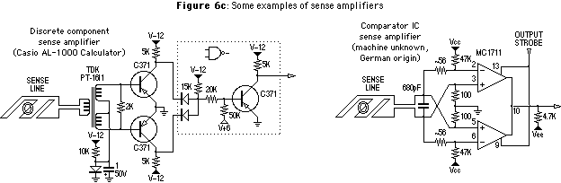
Sense amplifiers were constructed from either discrete components, standard voltage comparator integrated circuits or specialised ICs and generally include a STROBE input so that field reversals occurring when not sensing can be ignored.
Figure 6c shows some real-world examples.
|
|
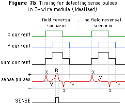
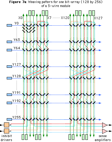
Observe that when reading a word the inhibit wire is not used as reading entails setting all the bits of a word to the same state, and when writing the sense wire is not used. The functions of the sense and inhibit wires can be combined into a single wire. Figure 7a shows the organisation of the X=128 by Y=256 bit-arrays used in a Burroughs 3-wire module.
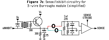
Note there are two inhibit drivers, sense amplifiers and sense/inhibit wires used for each bit-array. This is not really related to the 3-wire design, presumably it is a consequence of the large size of the bit-array producing noise issues beyond the capability of a single sense amplifier to tolerate. There are 32,768 cores in each bit-array of this module, so 16,384 cores per sense amplifier.
When sensing, the sense/inhibit (S/I) wire looks like the usual loop (see also figure 7c). It runs closely parallel to an address wire for blocks of 64 cores, but the transpositions of the S/I wire results in it parallelling the same address wire from the opposite direction for another 64 cores. For example, in figure 7a, an S/I wire (red segment) runs closely parallel to address wire X0 over the distance Y192 to Y255. The same S/I wire (blue/green segment) runs closely parallel to the same address wire over the distance Y128 to Y191, but is now coming from the opposite direction. Currents induced in the S/I wire from wire X0 thus cancel.
In addition, when sensing, the timing of the address current pulses appears to have been set such that the current on X-axis wires (parallel to the S/I wire) is turned on slightly before that on the Y-axis (perpendicular to the S/I wire).
A core field reversal will be triggered by the later leading edge of the pulse on the Y-axis.
Referring to figure 7b, current transitions on the address wires induce pulses in the S/I wire (X and Y pulses), the Y pulses being smaller because they result from the perpendicular Y-axis wire.
As the pulses are separated in time they do not sum and their level stays below the threshold for the sense amplifier.
A core field reversal produces a larger pulse (R), enough to trigger the sense amplifier.
|
|
When inhibiting, the S/I wire looks like two parallel elements. The sense amplifier ends are terminated with a low enough impedance to ground to permit the inhibit currents through (figure 7c). The paired alternation of the X-axis drivers matches the two 'inhibit elements' of the S/I wire. When an inhibit driver is activated, two cores on a given Y address wire will see inhibit currents. For example, suppose the core (X0,Y0) is to be inhibited during a write operation.
| Core (X0,Y0) will see currents: | (X=+1/2) | + (Y=+1/2) | + (I=-1/2) | = +1/2 |
| Core (X1,Y0) will see currents: | (X=0) | + (Y=+1/2) | + (I=-1/2) | = 0 |
Both cores are left in their current state, as is desired.
Another approach to a 3-wire system, referred to as 2-1/2 D system, is to weave only one of the address axis wires through the stack, and have separate drivers for the other axis of each bit-array (still at the cost of a lot more drivers).
|
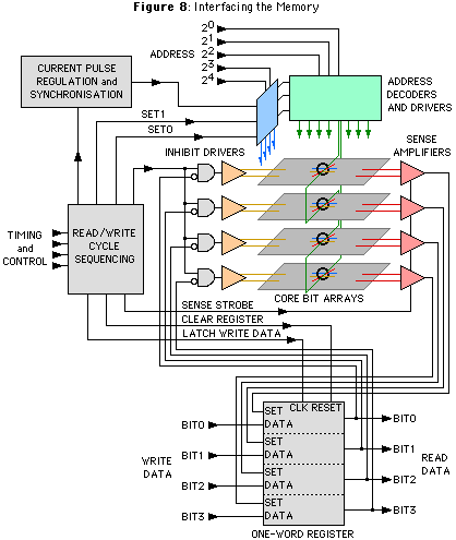
The read signals coming out of the sense amplifiers are very brief pulses corresponding to the field reversal of a core so they need to be latched into a register where they can be held for use (the one-word register in figure 8).
Reading a word is destructive - leaving all the cores (bits) in that word in the same state - so the data must be rewritten. When writing a word the first step will be to place the cores of that word into the same state so that some cores may then be changed to the other state while the remainder are inhibited from changing. Consequently a read cycle and a write cycle become almost identical operations:
As many computer instructions modify an operand in memory, and it would be wasteful of time to execute a full read cycle followed by a full write cycle, some systems incorporated a third type of cycle: the read/modify/write cycle, in which the data is read from core and modified by the CPU before being re-written.
Systems typically include a small state machine to generate control signals in the appropriate sequences for the various memory cycles.
Over the years the cores got smaller, switching times became faster, and array sizes increased. All this required tighter tolerances for address pulse timing and current levels. More sophisticated systems include circuitry for regulating and controlling these parameters. Temperature compensation of these parameters may also be included as characteristics of the ferrite core material change with temperature.
Core memory is non-volatile (does not lose it's state when powered off) and many systems took advantage of this feature for system recovery or to simplify the boot procedure.
However, the destructive read produces a problem: data may be lost if power fails after the sense operation but before the data is re-written.
To deal with this, systems may include special circuitry to ensure the completion of a memory cycle when power-fail is detected.
A book from the 1950s [ref:6] provides the following examples of physical characteristics for cores:
Core sizes vary, some smaller ones having an outside diameter of only 0.08 inch and an inside diameter of 0.05 inch. Larger ones range up to 0.4 inch outside diameter, . . .Cores were reduced in size by another factor of 5 or so over the years, a Burroughs module from the late 1970s has cores of approximately 0.015 or 1/64 inches outside diameter.
. . .
The [sense pulse ranges] in amplitude between 50 and 75 millivolts. . .
. . .
Switching time ranges from 1 microsecond to 5 microseconds, depending on the type and quality of the ferrite core. Driving current ranges from 400 to 800 milliamperes.
Table 11 presents some physical details of actual core memory modules. These represent a wide range of practical core implementations. They don't get smaller than that required by a simple calculator, but they did get larger than the 655,360 cores of the Burroughs module, on the order of 2,000,000 cores in a planar array according to [ref:5].
Module here means a group of cores woven together with the same set of address wires, together with their support circuitry. Memory systems of larger storage capacity were of course constructed from multiple such modules.
| ||||||||||||||||||||||||||||||||||||||||||||||||||||||||
| Top | bhilpert 2003 Dec |