| bh | PDP-11/HACK |
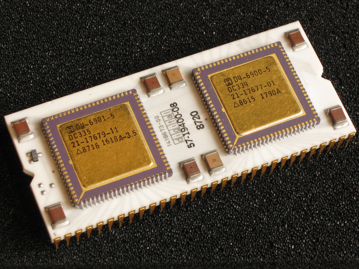
Some time ago a friend handed me a bare J11 chip. It had been pulled from some system on the way to scrap, presumably just because it was a pretty object. I don't know how many hands it had been through before arriving in mine but a few pins were bent and it had not been static-protected. I wondered whether it was now anything more than a pretty object.
The J11 (more properly the DCJ11, aka "Jaws") was one of the last gasps of the PDP-11 - a CMOS microprocessor implementation of the PDP-11/70. It's two chips actually, mounted on a single 60-pin, over-wide, DIP ceramic carrier. The J11 was developed in the early 1980s and introduced in the PDP-11/73 in 1983/84. Although this was at the end of the heyday of the PDP-11, the J11 saw a relatively long production life, being produced till sometime into the 1990s. The unit here has a date code from 1987.
I had a recollection of hearing that these microprocessors had a monitor program built into the microcode. Documentation confirmed this - it's called ODT (Octal Debugging Technique), a simple ASCII-based console monitor. In theory, if one could appropriately wire up a UART to the J11 one should be able to talk to the ODT via a serial terminal. The question was what would be the minimal hardware setup that would accomplish this.
|
Contents (this page):
Sub-pages: |
References / External Links: |
 The initial PDP-11/HACK breadboard setup. The J11 straddles two breadboards as it is too wide for a single breadboard. Baud-rate generator on circuit board at top. |
 8KW of memory added, as well as RESET and HALT switches. |
 Some basic ODT interaction. The "@" is the ODT prompt. An "R0" command begins the display of registers. Further on, The "0" command entry begins examination of memory at address 0. All numbers are in octal. |
 Entry and execution of Test #2 to output a stream of characters to the console display. The "10g" command entry begins execution. After some output of Bs, the HALT switch was pressed to take us back to ODT. ODT informs us execution has been halted at address 000016. |
The PDP-11/HACK is a minimal system built around the J11, enough to talk to the ODT, check the chip for basic operation, and enter and execute simple programs. Implemented with just 12 or 13 ICs, it has 16 KB of memory and a single I/O device: the console serial port. I'll hazard a guess this is the lowest-IC-count 'real' PDP-11 system - that is, leaving aside emulations on modern system-on-a-chip hardware or FPGA implementations. File it under silly-chip-tricks.
Thankfully, a datasheet for the J11 is available online at bitsavers.org. In short: a little reading of the J11 User's Guide, a little designing, a little breadboarding, and voilà: a functioning PDP-11. The schematic is linked above.
The ODT expects to see a 4-register device at addresses 17777560-17777566 in the I/O space. Normally this facility was provided by a DEC "DLART-compatible" device, DEC made the DC319-AA UART for the task. I didn't have a DC319 and I expect they're somewhat difficult to come by. Instead, I pulled a 6402 UART out of the parts bin, primarily because the 6402 is hardware configurable, so no boot-time programmatic access is required to load registers to configure it. The 6402 is also single-supply, making it mildly preferable over other hardware-configured UARTs such as the 1402 or AY-5-1013, although they too should do the job.
Just a few TTL gates were needed to make the 6402 appear on the bus as the 4 device registers with enough functionality to make the ODT happy.
The small PC board seen at the top in the breadboard photos is a baud-rate generator from some unknown piece of equipment, used here for the UART serial clock.
Something simpler could be done with just one IC, such as a CMOS 4060.
A
A couple more TTL chips were needed for an address latch for the multiplexed data/address lines and some bus protocol. The BS0/1 lines from the J11 do some pre-decoding to distinguish memory and I/O bus operations. This considerably simplifies the external address decoding required.
The first version had no memory, but it talked to the ODT and was enough to show the chip was working at some level. Next, two 6264 8K*8 static RAM chips were added to provide 8KW/16KB of memory. Two simple test programs were manually assembled, entered via the ODT and successfully executed (once I had reacquainted myself with the PDP-11 instruction set to the point of recalling that branch offsets are relative to the following instruction, not the branch instruction).
There is a little confusion around the maximum clock rate for the J11.
The 1983 Preliminary User's Guide specifies a max clock rate of 15 MHz.
Bob Supnik's article (link above) suggests they were achieving only around 4.5 MHz in that time frame.
Other sources indicate that later units went to 18 MHz.
The 11/HACK ran with crystals of 2, 4, 8 and 11 MHz, but did not function with a 14 MHz crystal though the on-chip oscillator was still going.
The limit is likely more a consequence of the rest of the system rather than the J11.
Note that while ODT will run while HALT is asserted, HALT must be deasserted prior to executing a program.
Before running a program, ensure the PSW is appropriate via the RS command. 000340 is typically good.
All numbers in the following are expressed in octal.
;**************************************************************************
;***	PDP-11 Test #1 - Increment R5 and return to ODT

000	005205			INC R5
002	000000			HALT


;**************************************************************************
;***	PDP-11 Test #2 - Repeatedly output a character to the console port

010	032737		loop	BIT #200,@#177564	; check bit-7/ready of xmt status reg
012	000200
014	177564
016	001774			BEQ loop		; busy-loop while bit-7 is 0

020	012737			MOV #102,@#177566	; send ASCII B to xmt data reg
022	000102
024	177566
026	000770			BR loop			; go send character again
2016 Dec:
Advisory: Note there is a flaw in the 11/HACK design regarding byte-write instructions.
Byte-write instructions will overwrite the 'other' byte of the associated word with unknown data.
To correct this, additional logic would be needed to recognise a byte-write via the J11 AIO lines and use LA0 to limit the write to only one of the memory chips.
(cf: DCJ11 User's Guide, sections 2.2.2 (pdf.33) & 3.6 (pdf.51)).
| Top | bhilpert 2014 May |