The new timing system breadboarded. |
|
|
Simon2006E uses only 'ordinary' relays, no special types are required. The stepper switch of the original has been replaced with ordinary relays. This leaves the paper tape reader as the only non-standard part to source.
The number of functional relays in the design is 66. As with the original design, some of those relays need more contacts than one is likely to find in a single physical relay. Multiple physical relays with their coils connected in parallel are used in such circumstances. For physical relays with a maximum of 4 double-throw poles, the total number required is 80. (See Misc. page of the schematic). This is down significantly from the 120-or-so of the original design, even with the timing stepper replaced with 13 new relays. The reduction is the result of some optimisation and of using more diodes in the logic than the original design. Simon2006E uses 86 logic diodes, the original uses (at least) 30.
At this time (2006 Sep) Simon2006E is a design exercise - I have not actually produced a complete physical implementation - so cannot testify to it's absolute correctness. However, the new timing system has been tested in physical form and the entire design has been simulated at the level of logical equations for the relays. The breadboarded timing system is shown in the photo, it ain't pretty but it works.
| Contents (this page): | Schematic (new window): |
| Relay Logic |
|
The electric/industrial convention of drawing contacts is used in the schematics here, those are not capacitors in the drawings.
| Architecture |
|
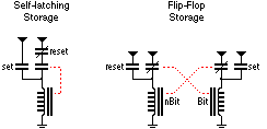
For storage the self-latching circuit is predominant in Simon, the exception being the carry register implemented as a flip-flop. The Simon2006E design just about eliminates switching relays.
Notice that CR4 does not exist in the physical implementation.
Taking advantage of the unspecified results of loading CR4 from other than IR and of using CR4 as a source, it is possible to eliminate the physical storage for CR4.
ER11 effectively implements the function of CR4, controlling the loading of the ALU result into CR5 and CY when CR4 is specified as the destination register in an instruction.
| |||||||||||||||||||||||||||||
| Timing |
| ||||
The design for the new timing system is presented in the schematic. Figure 3 shows the timing signals and what they accomplish.
The basic timing sequence is generated by 10 relays connected as a 10-stage ring counter. To clock the ring counter a trigger signal (Øa) and it's inversion are required. Note that the ring counter advances on both positive and negative edges of the trigger. A 50% duty-cycle is desirable for the trigger, otherwise alternate steps would have different periods. The Øa and Øb relays take a clock signal at 1 pulse per step with arbitrary duty cycle (Ø) and divide it by 2 to give a signal with 50% duty cycle.
Of course, if one uses a clock source which provides something close to a 50% duty cycle, the Øa and Øb relays can be eliminated.
The ring counter and drivers have been implemented and tested. Using some old relays I was able to clock the ring counter up to about 18Hz. Coincidentally, in the first R-E article an approximate instruction execution period of 2/3 second is mentioned, which equates to a step rate of 15Hz.
I have yet to arrive at a design for the oscillator for the clock. While trivial to implement with today's technology, it would be nice to have a design consistent with the period which avoided the complexity of tubes. One solution would be a small motor driving a cam and electrical contact.
One instruction is executed in one machine cycle. Only 9 steps are actually required for the machine cycle, so 1 of the 10 steps is wasted.
Processing of each element of a tape instruction triplet occupies 3 steps of the machine cycle including the stepping of the tape. The 3 steps for each element may be described as follows:
Referring also to the instruction encoding,
one can see from the timing diagram how the designers assigned the order of the instruction operands to the tape triplet elements to fit the execution of the instruction.
| The ALU |
A complete schematic for the ALU - including function decoding, circuits for the other ALU functions, and carry flag handling - was not presented in the R-E articles.
The completed Simon2006E ALU design is presented on the ALU page of the schematic. The basic structure is readily apparent. The lower 3 bits of CR4 are first decoded to 1-of-n lines to select the function to be performed. The function select lines feed groups of contacts from the operands which implement the logic for each function for each of the two bits of the result and associated carries. The function logic then feed the relays of registers CR5 and CY to store the results. Diodes prevent back-feed along the function logic output lines.
Note that while CR5 is implemented with relays in the typical self-latching configuration, the carry register is implemented with two relays interconnected as a flip-flop. This simplifies the timing design as the carry register does not have to be pre-cleared. (The decision to pre-clear CY could not be made until the function is known.) It does add the requirement that both carry and not-carry signals must be generated, however those signals are already present in the adder design.
The Simon2006E ALU has been optimised to reduce the number of contacts required. In the schematic, the circuit for bit 1 is shown un-optimised as it better represents the functional intent. The circuit for bit 2 is shown optimised: numerous contacts have been replaced with diodes which then feed into a single equivalent contact. The tally of contacts and relays presented in the schematic is based on both bits being optimised.
(Note: In the articles the ALU was referred to as the "computer circuits".)
| ||||
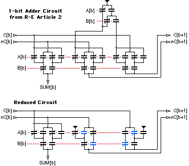
Two versions of an adder circuit are shown in figure 4. The first version is the circuit presented in the second R-E article. As suggested in the article, this circuit can be simplified. Such was done to arrive at the second version, which is used in Simon2006E. The notable aspect of these circuits is the way both carry and not-carry signals are propagated in-to and out-of each bit with no additional intervening relays. A solution using intervening relays would require additive settling time for those relays (ripply-carry propagation), although it would have the benefit of requiring fewer contacts. For the solution shown, the outputs are valid as soon as the operand contacts have settled.
In fact, even in the second circuit four of the contacts (blue) are not necessary to implement the actual logical requirements - they could be shorted over.
They are necessary to prevent back-feed however.
Diodes are not used for back-feed prevention here as they would increase the diode depth (discussed below in the power supply section).
In all four cases there is a complementary N.O. or N.C. contact, so assuming double-throw contacts, no additional relays are required.
| Power Supply |
The R-E articles do not present the schematic for the power supply. Mentioned in the articles and shown in the photos of Simon is a meter for the power supply. Initially I wondered why to bother with this as relays tolerate quite a wide variation in supply level so the power supply should be very simple.
While experimenting with the new timing system implementation, however, I found that at higher speeds the level can become critical. Basically, as the supply voltage is increased the response time for the relays increases, presumably due to the inductively stored energy in an activated relay increasing the time it takes for the relay to release. As the clock rate is increased then, the maximum permissible voltage level is reduced, and - together with the minimum pull-in voltage for the relays - the acceptable range for the supply voltage narrows.
Consequently, being able to adjust the supply voltage is beneficial or necessary to achieving the maximum clock rate for the system. A modern adjustable regulated supply could of course be used. Resistive techniques using rheostats may be a problem as the supply voltage would then vary with the state of the machine (number of activated relays). A small variac on the primary side of the power supply transformer may be the nicest solution consistent with the period.
This voltage/timing association also has some implications for the design of the logic. The voltage drop across backfeed-prevention diodes results in reduced voltage to the relays supplied through those diodes. The minimum supply voltage must consequently be raised in accordance with the maximum number of diodes in series in the system. Other relays see the higher voltage and are slowed in response time, thus reducing the maximum permissible clock rate. It is desirable then to keep the number of diodes in series, or diode depth, to a minimum. Although Simon2006E uses more diodes than the original, the diode depth is kept to a maximum of 1.
Simon2006 versions:
|
Machine Definition
| Relay Implementation
| Programs
| Simulation
| Alterations
Simon |
bhilpert 2006 Sep |