| bh | Univac Core Memory Module |
|
|
| Intention: | 32,768 words × 20 bits (18 data, 1 parity, 1 spare) |
| Gross Size: | 655,360 bits (cores) |
| Gross Size in Bytes: | 81,920 bytes |
| Gross Array Dimensions: | 1280 × 512 cores |
| Planar Dimensions: | 20 × 8 sense-arrays |
| Sense-Array Dimensions: | 64 × 64 cores |
| Scheme: | 2½D, 3-Wire |
| Physical Dimensions: | 26in × 20in × 4in ~ |
| Manufacturer: | Sperry-Rand/Univac |
| Computer: | UNIVAC 1108 (presumed) |
| Design Date: | 1964 (based on 1108 computer) |
| Manufacturing Date: | 1971 |
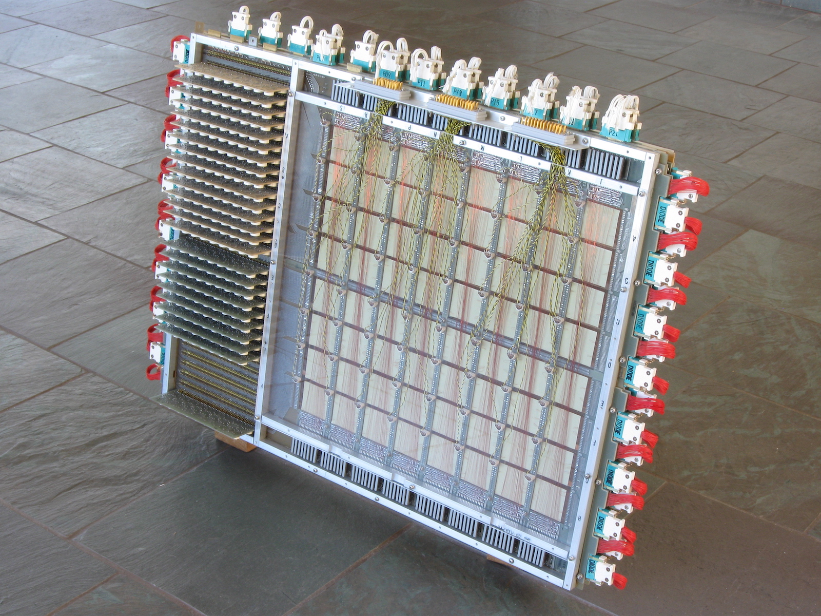
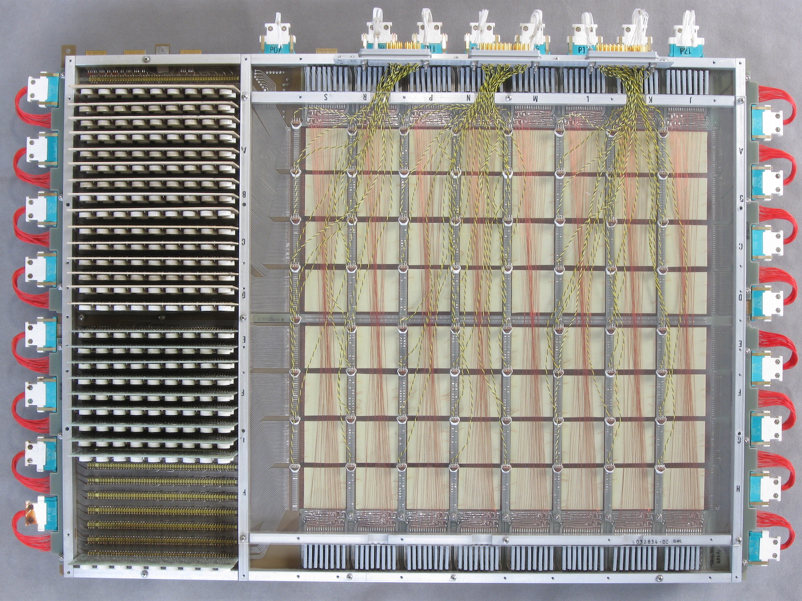
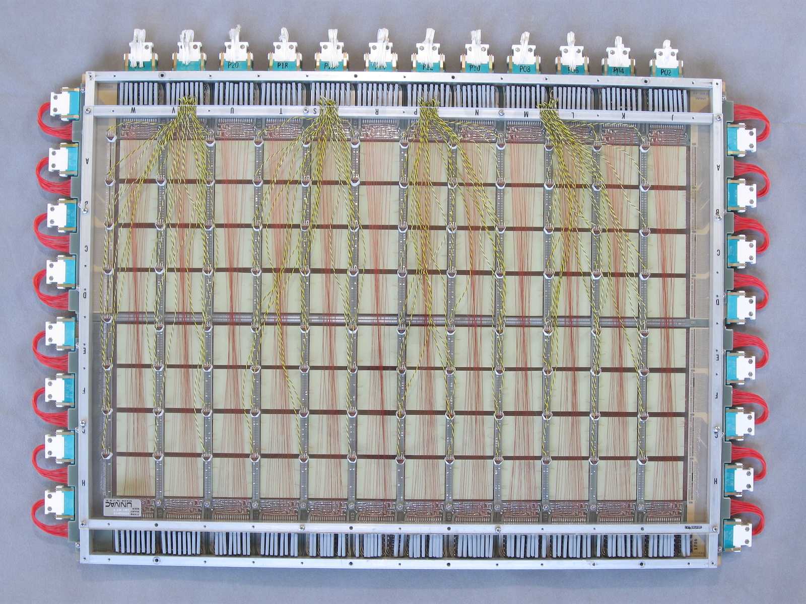
This is a large core memory module from a UNIVAC mainframe, manufactered in 1971. For technical interests, this module is interesting and notable for using a 2½D, 3-Wire organisational scheme.
The module contains the core arrays and some passive portions of the decoding/driving circuitry. The active address decoding and drivers are not present and no documentation describing them has been encountered, so the precise organisation of the address decoders and drivers is not known. In the reverse-engineered schematic a decoder-driver organisation-in-principle is described, based on what can be derived from the core module. The sense amplifiers were also external to the core module.
| CONTENTS (this page): | SUB-PAGES: |
EXTERNAL REFERENCES:
|
| RELATED: |
 |
 |
The model of machine this module belongs to has not been confirmed but some investigation suggests it was likely the UNIVAC 1108, or the 1106:
The UNIVAC 1108 was announced in 1964.
The 1108 was superseded by the 1110, announced in November 1971.
This module was manufactured in June of 1971 (from a date stamped on the module), so while late in the 1108 production period, still within that period.
[ref: History & Evolution of 1100.., pg.12/pdf.15]
The 1108 was a 36-bit machine, a half-word would be 18 bits. The raw word-width for this module is 20 bits but one bit was apparently a spare, leaving 19 bits: 18 bits with a parity bit.
The 1970 "1108 System Description" describes the 1108 as expandable in 32,768 word modules.
While this core module is 32,768 half-words, it may be that an expansion module was two core modules together with decoder/drivers and sense amps.
The document specifies each half-word indeed has a parity bit.
[ref: 1108 System Description,pg.3-1,2/pdf.23,24]
As mentioned, this module uses a 2½D scheme.
A 1990 history of Univac 1100 systems indeed mentions that the 1108 core memory used a "new" 2½D scheme.
[ref: History & Evolution of 1100.., pg.13/pdf.16]
 |
A derivative of the 1108 implemented in the same basic hardware - the UNIVAC 1106 - was introduced around 1969. The 1100 history document mentions the memory in the 1106 was altered from the 1108 [ref: History & Evolution of 1100.., pg.14/pdf.17]. If this alteration were still consistent with the 1108 design, it would be conceivable this module was from an 1106 with the essential design still originating in the 1108. Perhaps though, the alteration was redesigning the memory modules using a newer 3D,3-Wire scheme, which would not be consistent with this module.
The UNIVAC 418 was an 18-bit system introduced in 1962.
The last model in the 418 series - the 418-III - with the largest memory capabilities, was introduced around 1969.
According to a 418-III processor manual, the memory came in 16K modular increments made up from 4K sub-modules and had a parity bit for each 9-bit half-word, and so would not be consistent with this module.
[UNIVAC 418-III Process Reference, pg2-1/pdf.7]
 |
 |
 |
 |
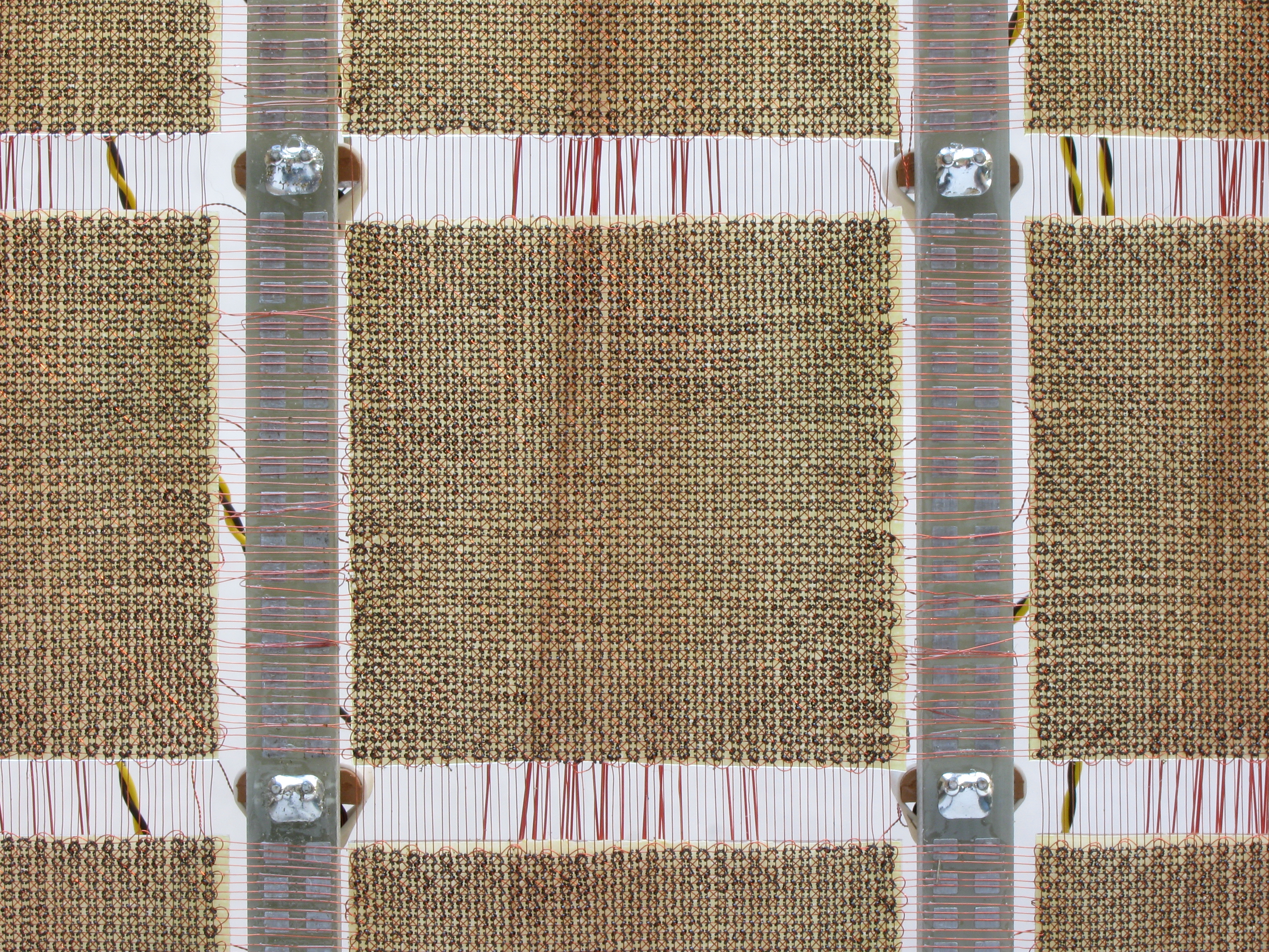
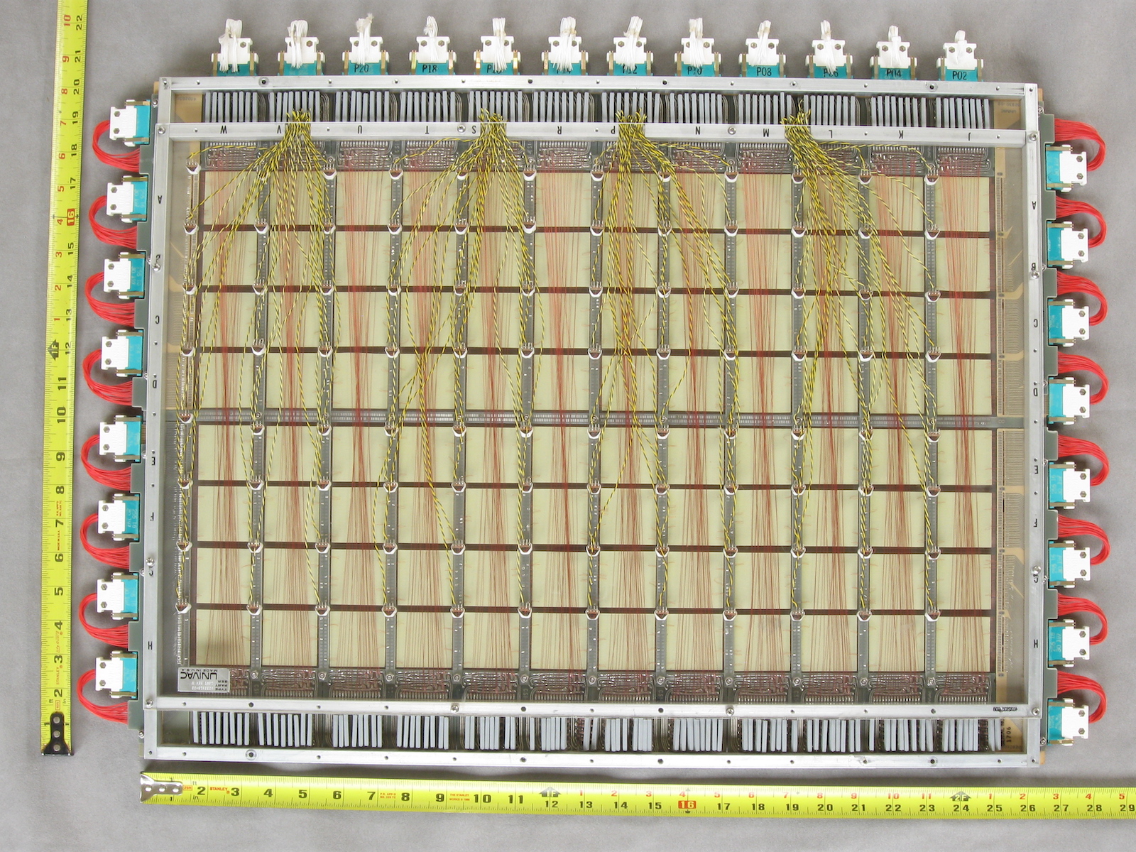
In the 2½D core memory scheme, the address space is divided into a 2D matrix with coincident-current addressing used on the two axes. Multiple bit-arrays as a 3rd dimension are present to form words, with shared drivers between bit-arrays on one of the addressing axes. However, the other addressing axis does not share drivers, instead each bit-array has its own set of drivers with data-control on these drivers to isolate control of each bit of a word when writing. This avoids the need for an inhibit wire woven through the core array, though at the expense of more drivers.
While 2½D memories can be implemented with just 2 wires through each core, in this design each core has 3 wires threaded through it:
The overall core array is 1280×512. The 512-wire Y-axis (horizontal wires in photos) is the shared axis, wires on this axis run through all bits of a word.
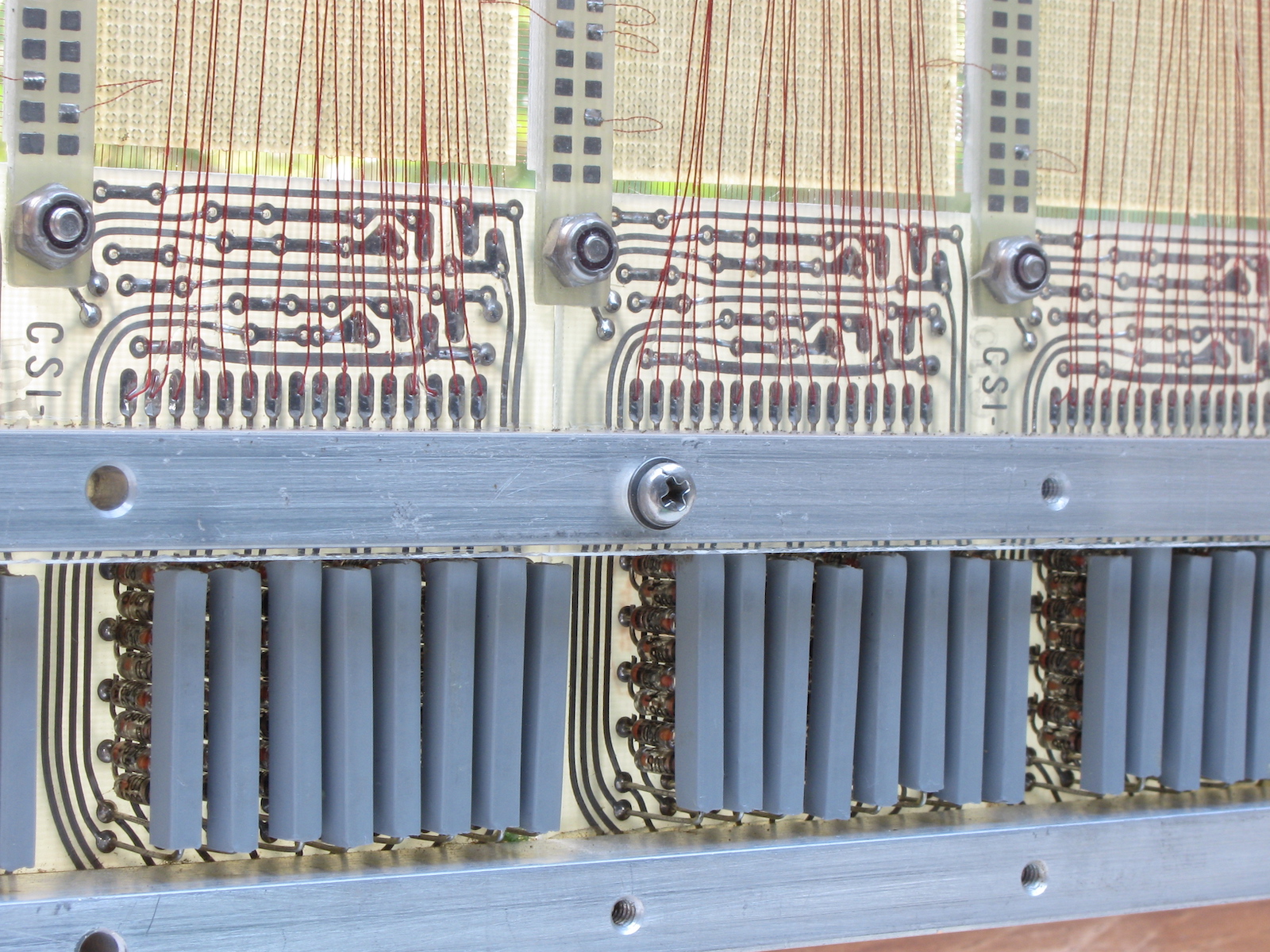
The 1280-wire X-axis (vertical wires in photos) is broken into 20 groups of 64 wires. This grouping delineates the bits of a word, that is, each sub-array of 64 horizontal × 512 vertical is one bit-array. Each set of 64 wires has it's own independant set of drivers.
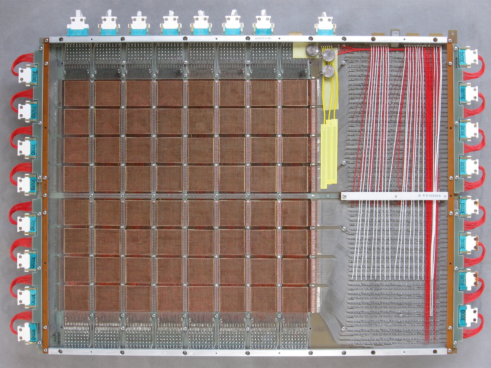
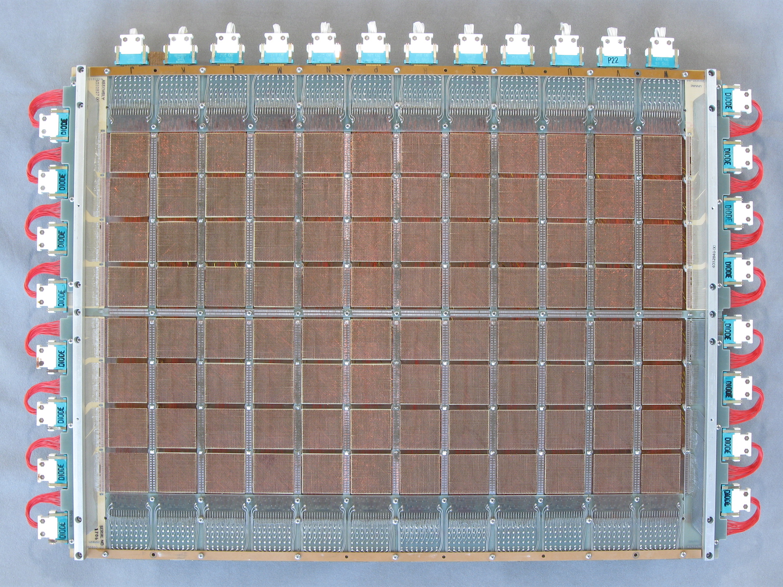
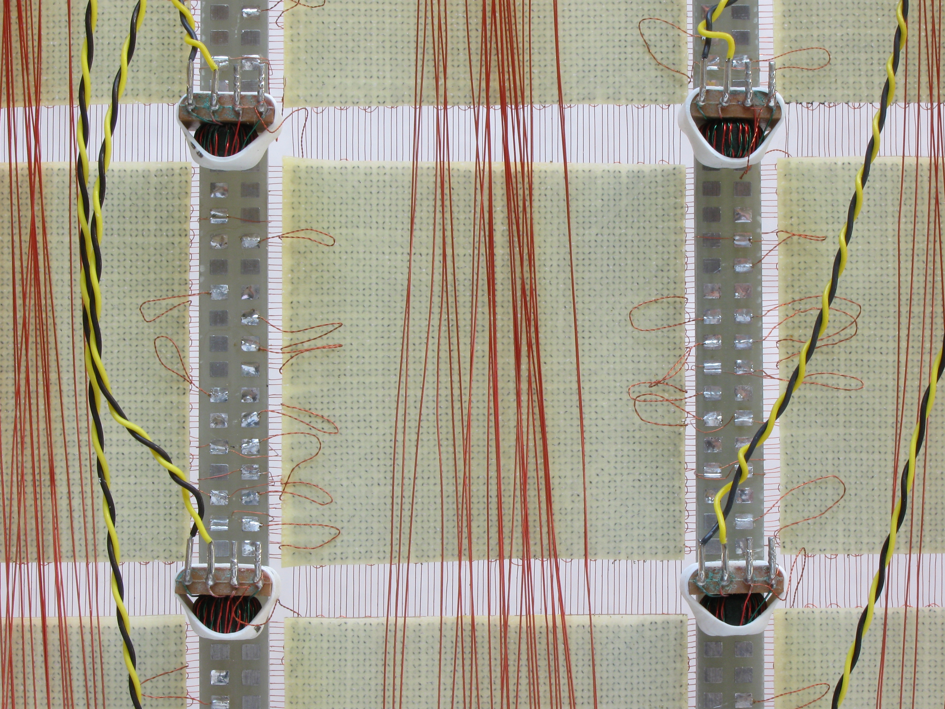
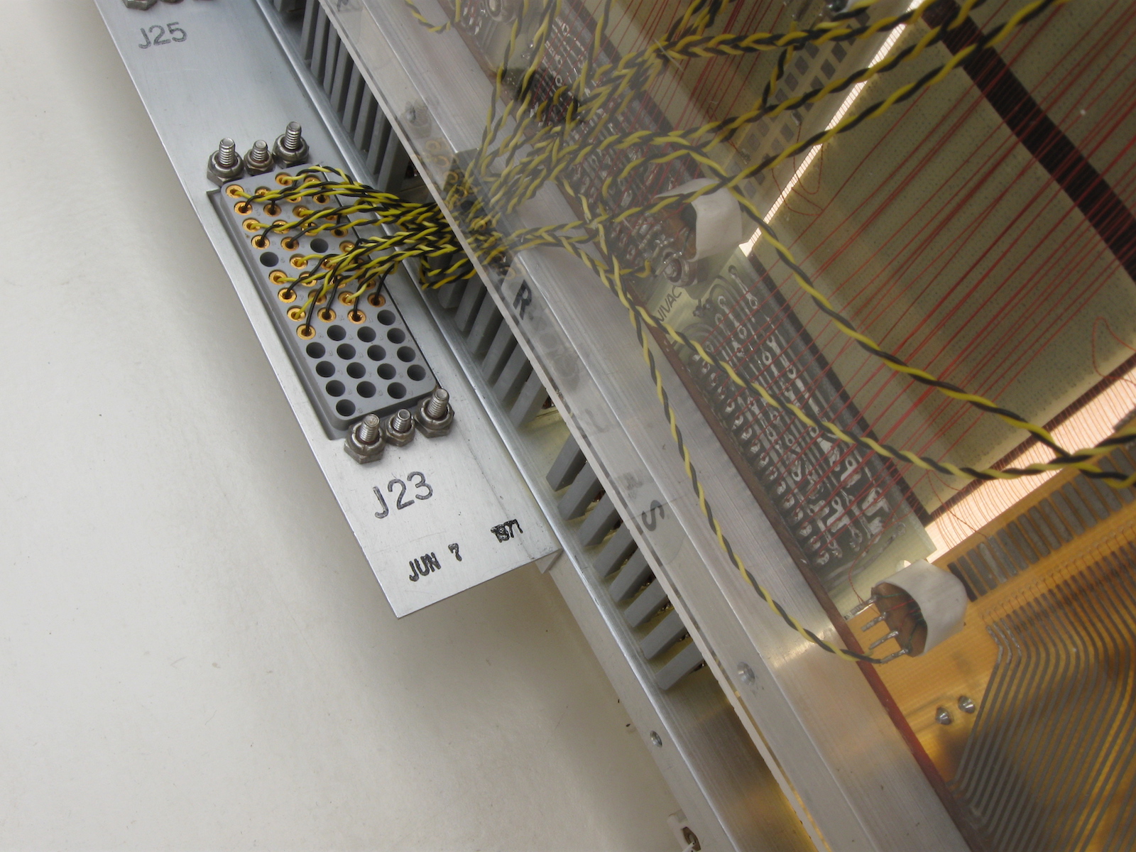
The cores are arranged physically as a 20×8 planar array of sense-arrays, though split and folded into a 2-level stack of an 8×8 frame and a 12×8 frame. The frame containing the 8×8 portion also holds a pulse-transformer decoding matrix for driving the 512-wire shared Y axis.
One of the 20 bit-arrays was apparently unused and was presumably present as a spare, this being the bit-array on the 8×8 frame nearest the decoder-matrix boards:
|
 |
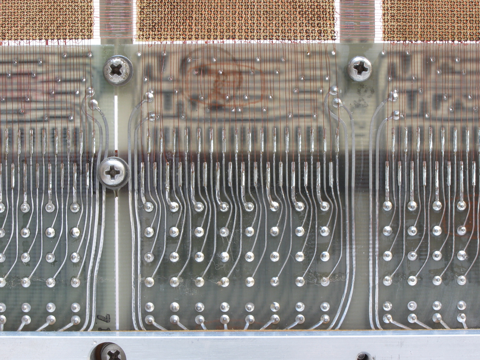
While there are functionally 20 bit-arrays of 64×512 cores each, there is a further division in that each bit-array is split on the 512-wire Y-axis into 8 sense-arrays of 64×64. An independant conventional diagonal sense wire threads each of these sense-arrays.
When reading, 1 of the 8 sense-arrays of each bit must be selected for monitoring. This was likely done by analog diode-switching of the sense pairs, such as was done in the AGC core-rope memory, the switches being then controlled by a 1-of-8 decoder fed by the 3 address bits of the Y-axis corresponding to the 8×64 grouping of the sense arrays.
Most of these splices are in the diagonal sense wire, though there are also a few splices present on Y-axis wires.
Each sense-array has at least 4 splices in its sense-wire.
Many have more, one has 11 splices.
This makes sense inasmuch as the diagonal sense-wire would have been by far the most difficult to thread in comparison to the X and Y axes wires.
 Note date code of 7128 (lower-left corner). |
 |
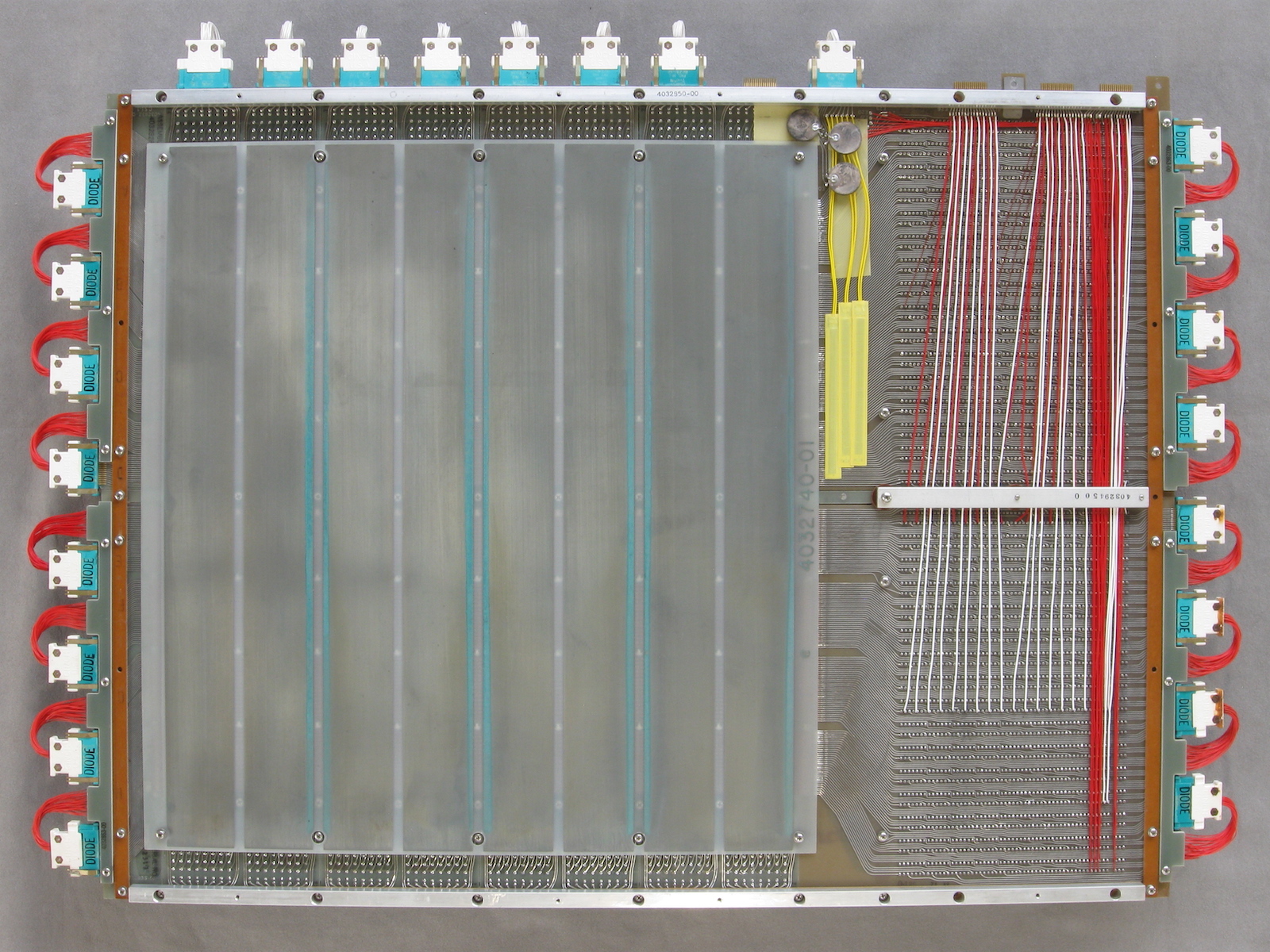
The first matrix is an 8×8 array of pulse transformers, both axes of this matrix are fed by active drivers. These drivers must drive current bidirectionally for reading versus writing.
The second matrix is a 8×64 array of pulse transformers. The 64 secondaries from the first matrix drive the 64-wide axis, the 8-wide axis is fed by drivers that simply close a circuit between the source secondary from the first matrix and a vector of destination primaries of the second matrix via ground.
The 8×64=512 secondaries from the second matrix then each directly drive one of the 512 Y-axis wires.
Taken together then, there are 3 sets of 1-of-8 inputs to these matrices. For each of these sets, 3 bits of address must be decoded to 1-of-8, thus 9 bits of address total, and of course 2^9=512.
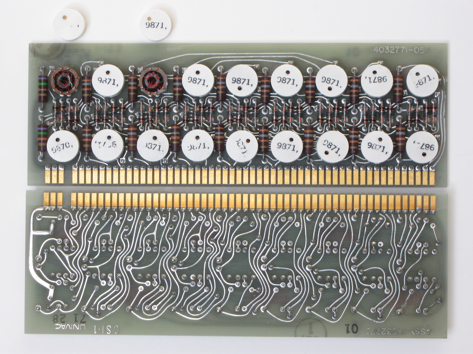
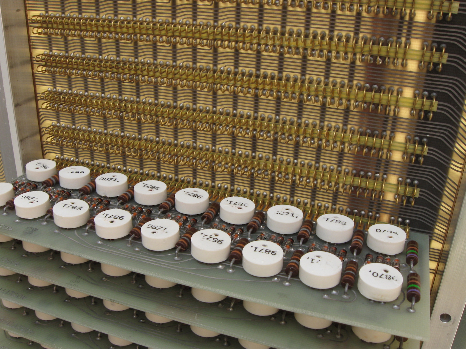
The two matrices are implemented on the 32 plug-in circuit boards. Each board contains two nodes from the 8×8 matrix, with each of those nodes driving an 8-node vector of the 8×64 matrix. Each board then, drives 2×8=16 wires on the shared Y-axis of the core array.
In the decoder-matrix board photo, the 2 left-most pulse transformers (type 9870) are the 2 nodes of the 8×8 matrix, the remaining 8 transformers of each row (type 9871) are each a vector of the 8×64 matrix.
There is some additional complexity in the wiring arrangement between the two 8-node vectors of each board in that there is a crossover between the two vectors for reading vs. writing [see schematic]. The point of this is not entirely clear but perhaps had something to do with noise reduction or driver current distribution.
Note that the drive energy for the shared Y-axis core wires all enters from the drivers of the first decoding matrix,
and must traverse through two pulse transformers to arrive at the cores.
 |
 |
Driver requirements for this 8×8 matrix could be 8 push-pull drivers with separated outputs to drive into the diodes of one axis, plus 8 push-pull drivers for the other axis. The decoder-driver combination for one of these axes requires an enable input for the data-bit control when writing to the bit-array. In principle, the drivers for the other axis could be shared across all the bit-arrays, though whether such a second level of shared drivers (in addition to the core array Y-axis sharing) was implemented is not known.
Two 1-of-8 decoders are needed, accounting for another 6 bits of address.
The number of address bits now totals 9+6=15, completing the word address space for the module: 2^15=32,768.
 |
 |
 |
 |
 |
 |
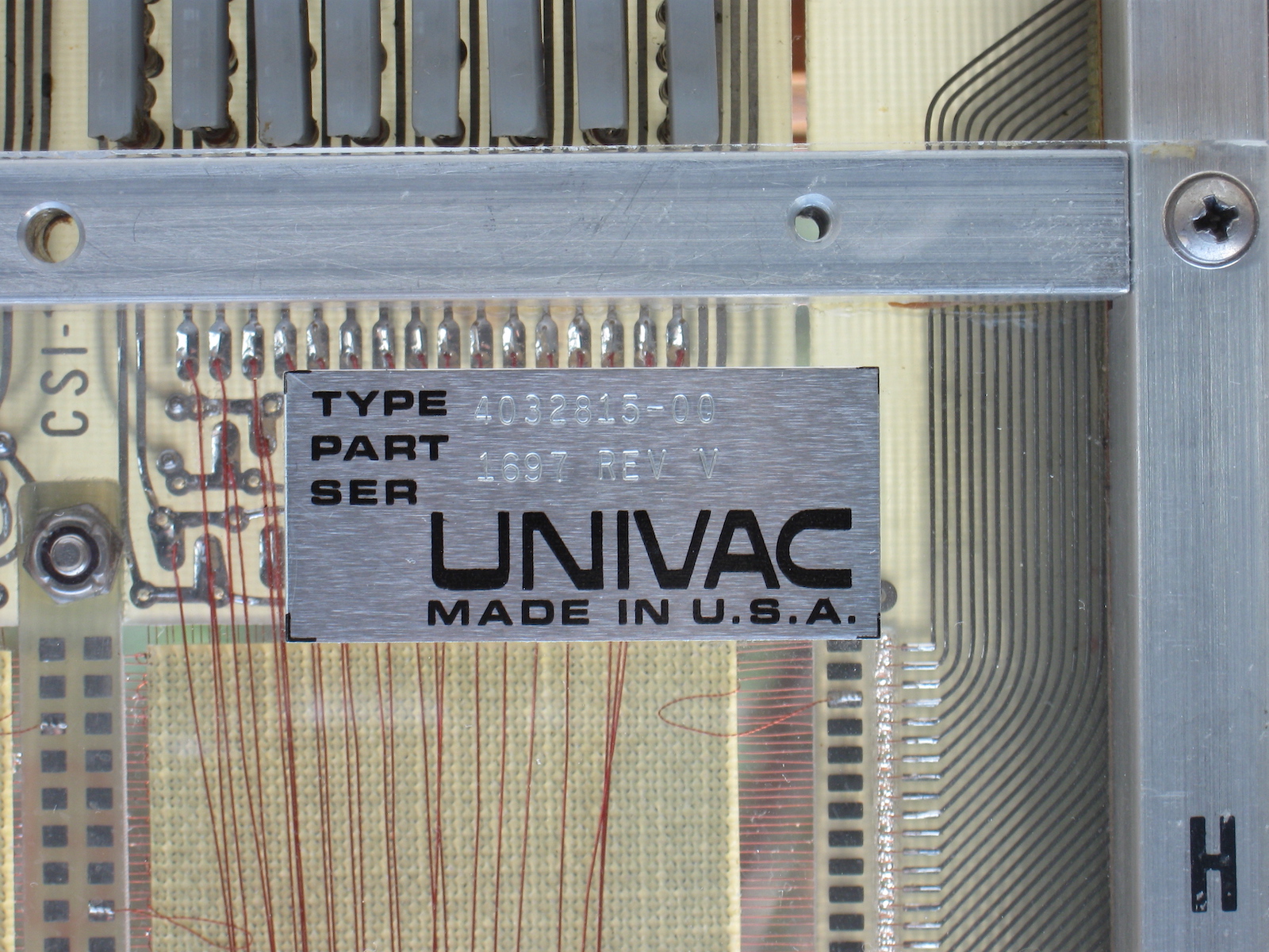
| Type: | 4032815-00 |
| Part #: | 1697 REV V |
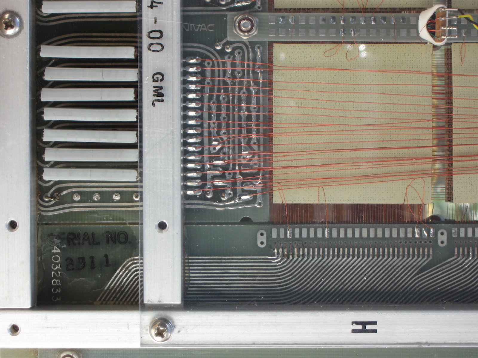
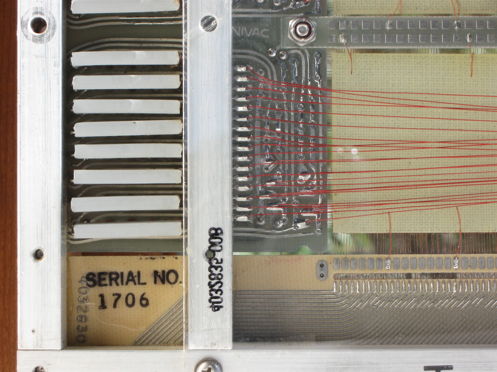
| Serial #: | 2311 (8×8 frame), 1706 (12×8 frame) |
| Univac Core Memory Module | bhilpert 2026 Apr |