|
|
Many calculators of Japanese origin from the late 1960s utilized integrated circuits from a family of ICs particular to several Japanese companies. Each of the manufacturers contributed a series with their own part numbers to the family but all are based on the same technology. In some cases the same IC was produced by more than one manufacturer but with different part numbers. Sometimes ICs from two or more of the series may be found in one calculator.
NEC and Hitachi seem to have gone through several revisions of their series, making improvements along the way.
Organisationally this is analogous to the situation in North America where manufacturers such as Fairchild, TI, National Semiconductor, etc. all produced series of TTL ICs which comprised a standard TTL family, although the manufacturers eventually converged on the common 7400 part numbers.
In the absence of any other name, "JMOS" has been chosen as a name for this family, for Japanese MOS.
Some of the ICs in this family, such as the TM4105 64-bit shift register, are (for the period and market) high density. Calculators built using this family ended up embodying two ends of the spectrum of technology: at one end utilising such high density devices; at the other, most of the gates in the calculators were still constructed from discrete diodes and resistors.
Contents (this page)
| Members of Family: |
NEC µPD1 Series NEC µPD10/100 Series Toshiba TM4000 Series Hitachi HD700 Series Hitachi HD3100 Series Mitsubishi M5800/M58000 Series Philco SC1772 |
| Period: | Late 1960s. Observed in application 1968 thru 1971. |
| Technology: |
Several factors indicate this family is MOS technology:
As it turns out, JMOS uses P-channel enhancement-mode MOSFET transistors. See the transfer curve below. (2021 Jul) |
| Supply Voltage: | -24V. A few devices require an additional -14V supply. |
| Logic: |
Gate symbols are presented in accordance with
Note though, that some calculators utilising these ICs are designed with negative logic, thereby reversing the above. AND and OR gate symbols should also be swapped. |
| Packaging: | TO-100 (10-pin) and TO-101 (12-pin) cans and standard DIP, depending on the date of production and the manufacturer. |
JMOS integrated circuits use a 2-phase clocking scheme for flip-flops.
They appear to be Master/Slave flip-flops with the clocks for the master and slave sections kept separate. In the EEC schematics these are referred to as:
The ΦC and ΦT inputs are driven by 2 out-of-phase and non-overlapping pulse streams. This made it possible to avoid the use of AC-coupled or edge-triggerred flip-flops which was common amongst others at the time.
Disadvantages are the additional connection to each flip-flop and the fan-out requirement of the driver for the ΦT pulse.
JMOS ICs were made for a narrow, internal market and for a short period of time. Finding replacements for failed JMOS ICs can present obstacles to the repair of calculators in need of such. Occasionally one may be fortunate to have or find an orphan board from which an IC may be re-used.
JMOS ICs also have a set of characteristics which are not readily replicable or substitutable by ICs of other logic families.
 It is possible however, to build functional substitutes for JMOS ICs from 4000-series CMOS.
4000-series CMOS ICs have a maximum supply voltage of 15-18V, lower than the 24V used for JMOS.
This necessitates both a supply reduction and level adapters at all inputs and outputs to the substitute.
It is possible however, to build functional substitutes for JMOS ICs from 4000-series CMOS.
4000-series CMOS ICs have a maximum supply voltage of 15-18V, lower than the 24V used for JMOS.
This necessitates both a supply reduction and level adapters at all inputs and outputs to the substitute.
The basic ideas are exemplified in the schematic to the right - a substitute design for a µPD10 (quad D-FF) - produced in 2000 for repair of a Toshiba BC-1212:
A similar approach was taken for a µPD105 (dual 16-bit shift register) for repair of a Riccar calculator in 2021. See the Riccar schematic for details.
A CMOS substitute was also used to regenerate a signal from a partially failed M5812 (6-bit ring counter) in the mentioned Riccar calculator.
In this case, the M5812 was functioning as 6 bits of a 16-bit ring counter for the digit timing.
One of the 6 outputs had failed although the rest of the IC and the ring counter as a whole were still working.
A circuit was designed using a 4013 to time off the other outputs of the ring counter to regenerate the one missing pulse output.
![]() Again in the Riccar calculator, a situation was encountered with two µPD13 ICs (5 inverters each) in which one inverter in each IC had failed.
Again in the Riccar calculator, a situation was encountered with two µPD13 ICs (5 inverters each) in which one inverter in each IC had failed.
As simple as the µPD13 is - a single PMOS transistor for each inverter - the JMOS transistor switching characteristics make it awkward to build a full substitute. The graph to the right shows the transfer curve for a PMOS transistor in a µPD13 IC. This characteristic curve makes for a nice logic transistor with a quite-sharp transition occurring at a voltage level providing decent noise immunity. However, with the transition occurring around -7V, it is not a characteristic readily found amongst the few discrete PMOS transistors available today.
In alternative for the Riccar, circuits were designed to use a bipolar PNP transistor to substitute for the failed PMOS inverters. Care in design must be taken in this approach, as the current-sense of the bipolar presents a very different expectation to the circuit than the voltage-sense of the MOSFET. As well, the base-current draw of the bipolar must be accounted for in a circuit not designed for it. The entire circuit of the PMOS inverter input - the driving output and all other inputs driven by that output - must be assessed as to the consequence of current draw for the bipolar base and the voltage levels seen in the driving circuit.
Bipolar substitutes were successfully prototyped for the two failed inverters, although in the end two µPD13s were recovered from an orphan board and used to replace the whole ICs instead.
(JMOS FET measurements from J. Ongena / 2021)
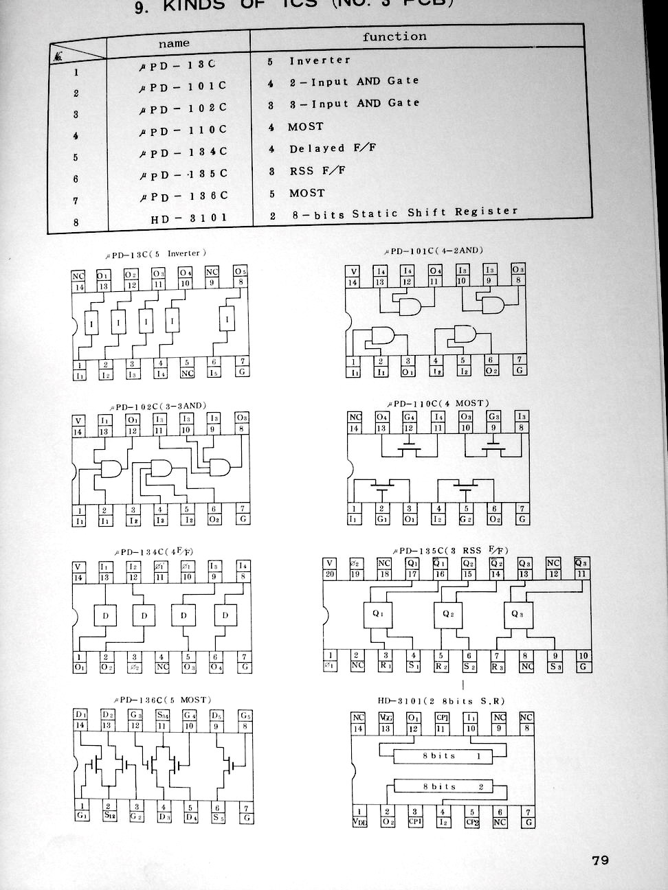
Twenty years after this web page was originally produced, original datasheets for some JMOS ICs were received. Following is an extract from an NEC 1969 Databook, covering some of the NEC µPD series ICs (from J. Ongena / 2021).
A few additional pinouts:
|
JMOS Family
Calculators | Integrated Circuits | Displays | Simulations EEC |
2000 Aug |