This page covers the hardware configurations of the three versions (A, B and C) of the 2116 processor.
An attempt is made to elaborate the similarities and the differences between the three versions.
It is not complete however, particularly with regards to the 2116A, for which I have little information.
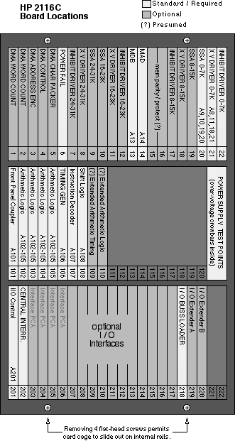
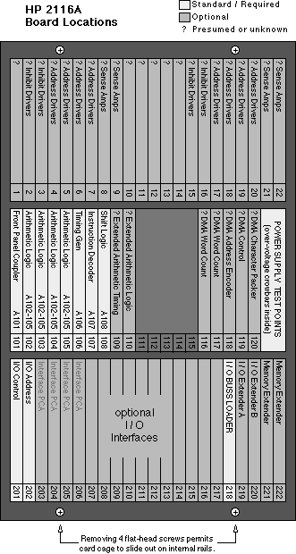
The three rows of boards in the 2116 cabinet are roughly delineated as:
- Top row: Memory
- Middle Row: CPU
- Bottom row: Input/Output
The three versions differ primarily in the maximum amount of memory which can be installed in the main cabinet, reflected most noticeably in the re-organisation between the versions of the top row of boards.
The A model contains up to two 4 KWord core modules while the B model contains up to two 8 KWord modules.
The C model contains up to four 8 KWord modules, the modules being different than those of the B.
Note that aside from the I/O interface slots, the backplane is not a bus architecture: a particular slot is intended to receive a particular board.
The I/O interface slots (203 thru 218) are a bus architecture, the only difference between slots being the select code assigned to the slot and consequent interrupt priority (lower slot number, higher priority).
The power supplies for the 2116s are relatively complex for 'simple' linear supplies.
There are various inter-dependancies between the regulators for proper power-up/down sequencing.
The construction of the main logic supplies of +4.5V and -2V is such that the +4.5V line is actually the regulator common and the regulators supply -4.5V and -6.5V.
Contents (this page):
Gallery
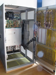
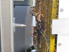
All photos are of a 2116C.
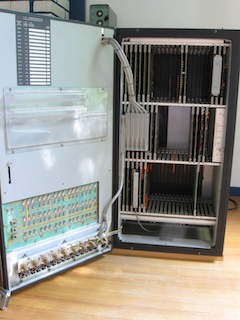
Opening the front door gives access to the card cage and allows for front panel lamp replacement.
There are also some test mode switches on the rear of the front panel.
|
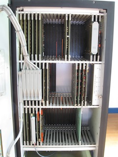
The card cage:
DMA & memory on the top row, CPU on the left of the middle row, and I/O on the bottom.
The 4 boards to the right on the middle row are just being stored there.
On the far right of the middle row are power supply test points.
|
The card cage slides out on 4 internal rails, the two left rails split and the cage then swings on hinges built into the two right rails,
giving access to the backplane wiring and the power supply.
|
The split rails on which the card cage mounts.
|
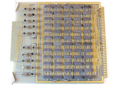
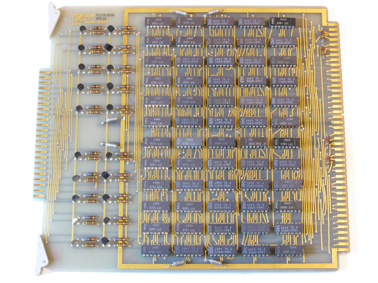
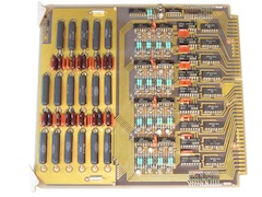
One of the CPU boards: a 4-bit slice of registers and ALU.
4 of these boards are present in the CPU for the 16-bit word-width.
|
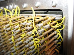
The backplane is wired with a type of crimp connector.
|
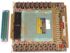
SSA: The planar-array of cores and the sense amplifiers of the 8KW memory module.
Jumper block to connect with the XY DRIVER board included on the left.
|

XY DRIVER: Address matrix drivers of the 8KW memory module.
Note the TO-19 transistor providing a fix for one blown transistor in a quad-transistor DIP package.
|
INHIBIT DRIVER: The third board of the 8KW memory module.
|
| |
|
2116A Configuration
The A version permits two 4 KWord modules to be installed in the main cabinet.
Each 4 KWord module appears to be composed of:
- 2 Sense Amplifier boards,
- 4 Address Driver boards,
- 2 Inhibit Driver boards,
- Core Stack: 4K core stack located behind the backplane.
Power supply voltages and primary usage are as follows:
| Voltage | Use |
|---|
| +4.5 | logic |
| -2 |
| ? | core X/Y drivers |
| ? |
| ? | core inhibit drivers |
| +12 | I/O line drivers |
| -12 |
|
Still much to find out about this model version.
2116B Configuration
The B version replaced the two 4 KWord modules of the A with two 8 KWord modules, made possible in large measure by the use of anti-coincident addressing.
Each 8 KWord module is composed of:
- 2 Sense Amplifier boards: each board has 17 sense amplifiers for 4K of core,
- 2 Driver Switch boards: 1 board drives the X lines for 8K, the other the Y lines,
- 2 Inhibit Driver boards: each board has 17 inhibit drivers for 4K,
- Core Stack: 8K core stack located behind the backplane. (The stack is actually two groups of 4K with one dimension of address lines flipped between the two groups for anti-coincident addressing.)
Power supply voltages and primary usage are as follows:
| Voltage | Use |
|---|
| +4.5 | logic |
| -2 |
| +22 | core X/Y drivers |
| -22 |
| +32 | core inhibit drivers |
| +12 | I/O line drivers, core sense amps |
| -12 |
|
2116C Configuration
The C version permits four 8 KWord modules to be installed in the main cabinet, however these modules are different than the 8 KWord modules of the B.
The core stacks at the back are gone, the core is now mounted on the regular plug-in boards.
Each 8 KWord module is comprised of 3 boards:
- SSA board (core stack and sense amps),
- X Y DRIVER board,
- INHIBIT DRIVER board,
- interconnect plug between the SSA and X Y DRIVER boards. Note there are two types of interconnect, for the different relative orders of the 2 boards. The 0-7K and 16-23K positions use interconnect part no. 02116-63244, while 8-15K and 24-31K use 02116-63243.
The lowest 8 KWord address range is covered in slots 20, 21 and 22.
I don't know the addressing order for the other slots.
The new memory modules are similar to those used in the 2100A, enough so that large portions of the schematic for the 2100A modules applies to the 2116C modules.
Note that because the maximum addressable memory (32 KWords) can now be installed in the main cabinet, the memory extender slots (221,222) are no longer needed.
Slots 15 and 16 are presumably for the memory parity and protection options (order not known).
The power supply was altered from that of the B for different voltages required by the new memory modules:
| Voltage | Use |
|---|
| +4.5 | logic |
| -2 |
| +20 | core X/Y drivers, inhibit drivers |
| -20 | core X/Y drivers |
| +12 | I/O line drivers, core sense amps |
| -12 |
|
The alterations focus around the removal of the +32V supply and increasing the current capacity of the +20V supply via use of the 'old' +32V filter capacitors.
There is also a change between the B and C models in the manner in which the line supply is switched on/off (push-button on the B, toggle switch on the C).
The majority of the schematic for the 2116B supply (2116B Vol. 2 pg. 5-91) still applies to the 2116C.
Board List
Following is a list of boards for use in the 2116A, B and C.
A "?" in the slot column for the model indicates that I do not know whether it is permissible to use that board in that processor model.
In most such cases there is another version of the board which is known to be applicable to that processor.
Note: I/O interface boards are listed on another page.
Note: "V Dat Dv" is Version, Date and Division.
|
CPU
|
| Name / Label |
Board Number |
Revision
V Dat Dv |
Description |
2116A Slot |
2116B Slot |
2116C Slot |
Refs |
| Front Panel Coupler |
02116-6184 | ? |
Difference from 6208 unknown. |
? |
101 |
? |
IB2 |
| 02116-6208 | D 942 22 |
|
? |
101 |
101 |
MB2.70,PBC |
| Arithmetic Logic |
02116-6026 | L 805 22 |
4-bit slices of the registers and ALU. |
? |
102-5 |
102-5 |
MB2.70,PBC |
| TIMING GEN |
02116-6281 | 923 |
|
? |
106 |
? |
MB2.70 |
| 02116-63220 | C 1043 22 |
Difference from 6281 unknown. |
? |
? |
106 |
PBC |
| Instruction Decoder |
02116-6027 | K 830 22 |
|
? |
107 |
107 |
MB2.70,PBC |
| Shift Logic |
02116-6029 | K 729 22 |
|
? |
108 |
108 |
MB2.70,PBC |
| Extended Arithmetic Unit Timing |
02116-6196 | ? |
Provides additional arithmetic instructions. |
? |
109 |
? |
IB2 |
| Extended Arithmetic Unit Logic |
02116-6202 | ? |
See above. |
? |
110 |
? |
IB2 |
| |
|
Memory
|
| Name / Label |
Board Number |
V Dat Dv |
Description |
2116A |
2116B |
2116C |
Refs |
| Memory Module Decoder |
02116-6300 | 937 |
Selects the addressed module. |
|
2 |
|
MB2.70 |
| 02116-6274 | 811 |
Selects the addressed module. (BACKDATED) |
|
2 |
|
MB2.70 |
| Direct Memory Logic |
02116-6069 | 907 |
Buffering, switching between CPU access and DMA access. In spite of the name, this board is required, even if the DMA option boards are not present.
|
|
20 |
|
MB2.70 |
| 02115-6044 | 821 |
Logic appears to be identical to 02116-6069, but bias/load resistors are different, this board uses CTL, 6069 uses CTL & TTL. (BACKDATED) |
|
20 |
|
MB2.70 |
| Sense Amp |
02116-6298 | 902 |
17 sense amps for 4K. |
|
10,11,
12,13 |
|
MB2.70 |
| 02115-6001 | 744 |
17 sense amps for 4K. (BACKDATED) |
|
10,11,
12,13 |
|
MB2.70 |
| Driver Switch |
02116-6266 | 943 |
Address drivers for 1 dimension of 8K. |
|
8,9,
14,15 |
|
MB2.70 |
| Inhibit Driver |
02116-6265 | 819 |
17 inhibit drivers for 4K. |
|
4,6,
16,18 |
|
MB2.70 |
| MDB |
02116-63248 | A 1018 22 |
Memory Data Buffer? |
|
|
13 |
PBC |
| MAD |
02116-63212 | A 1016 22 |
Memory Address Decoder? |
|
|
14 |
PBC |
| SSA |
02116-63207 | A 1035 22 |
8K core stack and sense amplifiers.
(also: 02116-83209)
(on core stack: 02116-63207 / B 1035 22 / 5087-1004)
|
|
|
9,10,
19,20 |
PBC |
| X Y DRIVER |
02116-63211 | A-1016-22 |
Address drivers for 2 dimensions of 8K.
|
|
|
8,11,
18,21 |
PBC |
| INHIBIT DRIVER |
02116-63260 | A-1042-22 |
Inhibit drivers for 8K.
|
|
|
7,12,
17,22 |
PBC |
| Memory Parity Check |
12591-6001 | ? |
Optional.
|
? |
3 |
? |
M13206 |
| Memory Protect |
? | ? |
Optional.
|
? |
21 |
? |
|
| Memory Extender |
02116-6181 | ? |
For connection to optional 2150A extender cabinet to provide additional memory.
|
221,222 |
221,222 |
|
BI2 |
| |
|
DMA
|
| Name / Label |
Board Number |
V Dat Dv |
Description |
2116A |
2116B |
2116C |
Refs |
| DMA WORD COUNT |
02116-6206 | C 908 22 |
The DMA boards provide 2 independant channels of Direct Memory Access for high speed I/O devices such as magnetic tape and disks.
|
? |
116,117 |
1,2 |
PBC |
DMA Address Encoder
DMA ADDRESS ENC |
02116-6205 | ? |
? |
118 |
? |
IB2,M13206 |
| 02116-6315 | B 936 22 |
? |
? |
3 |
PBC |
| DMA CONTROL |
02116-6204 | A 751 6 |
? |
119 |
4 |
PBC |
DMA Character Packer
DMA CHAR PACKER |
02116-6203 | ? |
? |
120 |
? |
IB2,M13206 |
| 02116-6313 | A 750 22 |
? |
? |
5 |
PBC |
| |
|
I/O Bus Support
|
| Name / Label |
Board Number |
V Dat Dv |
Description |
2116A |
2116B |
2116C |
Refs |
I/O Control
A201 |
02116-6041 | 640
710
L 839 22 |
Part of I/O bus interface with CPU. Global interrupt control. |
201
? |
201
? |
?
201 |
MA3.67,MB2.70
PBC |
| I/O Address |
02116-6042 | 651
703 |
Part of I/O bus interface with CPU. Select-code decoding & central interrupt register. |
202 |
? |
? |
MA3.67 |
I/O Address
CENTRAL INTERR. |
02116-6194 | na
C 829 22 |
Referred to by both names. Difference from 6042 unknown. |
?
? |
202
? |
?
202 |
MB2.70
PBC |
I/O BUSS LOADER
(sic) |
02116-6047 | 701
B 920 22 |
Termination resistors, should come after all I/O interface boards.
Not required if all interface slots (203-218) are filled.
|
218 |
218 |
218 |
MA3.67,PBC |
| I/O Extender (part 1) |
02116-6182 | ? |
For connection to optional 2150A extender cabinet to provide additional I/O slots. |
219 |
219 |
219 |
BI2 |
| I/O Extender (part 2) |
02116-6183 | ? |
See above. |
220 |
220 |
220 |
BI2 |
| |
|
Miscellaneous
|
| Name / Label |
Board Number |
V Dat Dv |
Description |
2116A |
2116B |
2116C |
Refs |
| POWER FAIL |
02116-6175 | D 925 22 |
Power fail detection and interrupt generation.
Also generates POFP (Power On-Off Pulse) and PON (Power On Normal) signals.
|
? |
1 |
? |
MB2.70 |
| POWER FAIL |
02116-6305 | D 925 22 |
This is a -6175 with a handwritten label on it saying it has been rebuilt as -6305.
One zener may have been replaced.
|
? |
? |
6 |
PBC |
| Power Fail with Auto-Restart |
12588-6001 | ? |
Appears to be an optional alternative to the Power Fail board. |
? |
1 |
? |
M13206 |
| |
|
Power Supply
|
| Name / Label |
Board Number |
V Dat Dv |
Description |
2116A |
2116B |
2116C |
Refs |
| Logic Supply Regulators |
02116-6014 | D 638 22
D 1049 22 |
Control for +4.5V, -2V, +12V regulators. |
? |
301 |
301 |
MB2.70
PBC |
| Memory Supply Regulators |
02116-6015 | D 822 6 |
Control for +22V, -22V, -12V, +32V regulators. |
? |
302 |
|
MB2.70 |
| 02116-63214 | E 1049 22 |
Control for +20V, -20V, -12V regulators.
Almost identical to -6015 but with the components for +32V left out.
(Also marked with 02116-8015.)
|
|
|
302 |
PBC |
| Crowbars PCA |
02116-6126 | D 837 6 |
|
|
121,2 |
|
MB2.70 |
| 02116-63213 | D 1009 22 |
Identical to -6126 but with the components for +32V left out.
(Also marked with 02116-8126.)
|
|
|
121,2 |
PBC |
|
Key to Refs:
- PBC: Physical board from my 2116C.
- MA3.67: Manual for 2116A, Vol. 3, 1967; from bitsavers.
- MB2.70: Manual for 2116B, Vol. 2, 1970; from bitsavers, esp. Pg. B-02/507.
- IB2: Class (Instructional) manual for 2116B, Vol. 2; from bitsavers.
- M13206: Manual in 13206 PDF from bitsavers, contains list of 2116B configs for 2000A systems.
Miscellania
- Power supply and backplane are accessed from front by removing 4 flat-head screws on black bezel behind front door and pulling out the card cage. Card cage is mounted on internal sliding rails.
- To access crowbars remove 6 flat-head screws on card cage, not round-head screws on crowbar cover.
- The two power supply regulator / heatsink modules drop down after removing screws behind the rear panel.
- Front panel lamps are CM 345. These lamps are specified as 40mA @ 6V, however they run under-voltage in the processor, which improves their longevity. The lamps in register-bit positions draw about 31ma @ 4.1V, the lamps in the push-buttons draw about 36mA @ 5.4V, as measured in a 2116C.
- Available: schematic for 2116C Power Supply.
- Available: schematic for X Y Driver board of 2116C 8 KWord memory module.
 This page covers the hardware configurations of the three versions (A, B and C) of the 2116 processor.
An attempt is made to elaborate the similarities and the differences between the three versions.
It is not complete however, particularly with regards to the 2116A, for which I have little information.
This page covers the hardware configurations of the three versions (A, B and C) of the 2116 processor.
An attempt is made to elaborate the similarities and the differences between the three versions.
It is not complete however, particularly with regards to the 2116A, for which I have little information.