1. Supply Voltages and Logic Levels
The main logic supply is +12V with:
- Logic 1 / TRUE = +12V
- Logic 0 / FALSE = 0V
A bias supply of -6V is also present to pull down the base of transistors and a supply of +20V is used to drive the core memory address and inhibit wires.
The +20V is also present on some gates and flip-flops leading to the core memory addressing.
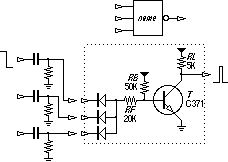
2. Gates
| |
Figure 2a: Simple Gate Construction
|
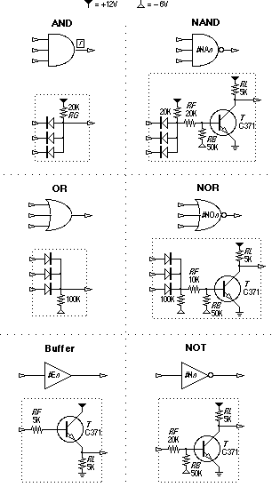
|
Basic logic gates are implemented from a form of Diode-Transistor-Logic, operating in a combination of current-sinking and current-sourcing modes, and constructed from discrete components, as shown in figure 2a.
Component values vary on occasion from those shown to accomodate particular drive requirements.
The most prevalent logic structure is AND-NOR. AND gates can drive a NOR gate directly, without buffering, as elaborated in figure 2b.
The AND gate inputs must be driven by a low impedance to ground as shown for one input.
Straight OR gates are used only a couple of times due in part to their limited current-sinking ability (high impedance to ground).
| |
Figure 2b: AND-NOR Elaboration
|
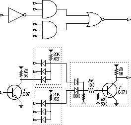
|
3. Bistable Flip-Flops
| |
Figure 3: Bistable Flip-Flop Construction
|
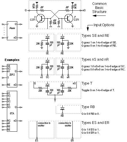
|
Today we most frequently deal with J-K and D type flip-flops.
When constructing flip-flops from discrete components however, some other forms were used to help reduce component counts.
In the AL-1000 all bistable flip-flops are based around the well-known structure at the top of figure 3 (again, some component values vary for particular circumstances).
There are several input types which can be applied to this common base, and multiples of these inputs and/or multiple combinations may be applied to a single flip-flop, as shown in the two inset examples.
Note that clock inputs are negative-edge triggered.
Latches are generally constructed from flip-flops with an RE input and an nS input.
The latch is cleared with the RE inputs before loading the desired data.
The desired data is loaded into the latch either by clocking the SC inputs with the inverted data on the nS inputs, or by holding the nS inputs 0 while the falling edge of the data bits which are 1 clock the SC inputs.
4. Monostable Flip-Flops
| |
Figure 4: Monostable Flip-Flop Construction
|
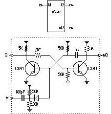
|
Two monostables are used in the AL-1000, one in the T state machine for keyboard debouncing and one in the power-on-reset circuitry.
5. Edge-Pulse Gates
| |
Figure 5: Edge-Pulse Gate Construction
|
|
'Edge-Pulse' gates are used in several places to convert a negative-going edge to a full pulse.
As shown in figure 4, these gates are fed by differentiating capacitors and resistors and are biased in such a manner that the input normally appears as 1 and the output 0.
A 1->0 transition at an input to a capacitor sends a differentiated negative-going pulse to the transistor, enough to briefly turn the transistor off so that a 1 pulse appears at the output.
The edge-pulse gates are used to slightly delay the negative edge of a signal for the following purposes:
- To avoid ambiguous or race conditions when clocking flip-flops (for example the clearing and loading of the D latch).
- To 'soak up' glitches which result from clock signals being gated through combinatorial logic. The glitches would otherwise result in multiple clocking of following flip-flops. As long as the glitches occur within the on-time of the edge-pulse gate, only one negative edge will be propagated out.