| HP 9830 | HP 9830 Hardware Architecture |
The 9830 was under development in the very early 1970s. Not surprisingly for the period, it is implemented primarily with 7400-series MSI and SSI TTL ICs, along with some bipolar ROMS for microcode, and early MOS ROM and RAM memory chips. It was a little too early for use of 74LS devices, but there are some 74H, 74L and 74S series ICs (high-speed, low-power and Schottky series). 512*8-bit MOS ROMs are used to store the firmware and 1K*1 1103 MOS dynamic RAM chips for read/write memory.
There are 77 different types of IC used. With 8KW of RAM there are a total of over 460 ICs.
As was common for Hewlett-Packard in that era, the printed circuit boards are gold-plated over all the copper, not just on the edge-connector fingers. Most of the boards are double-sided, although three are multi-layer: the LED display, RAM memory and M-register boards.
The full schematic may be referenced for greater detail relating to the following descriptions.
The number of bits processed in a micro-operation can be further affected by the microcode IQN bit and selected condition.
This does not affect the time period of the micro-cycle however, it just suppresses the shift clock.
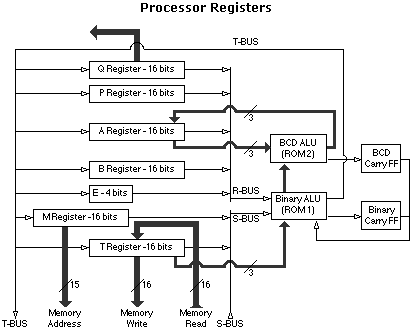
In general, during micro-operations, the specified source registers will be rotated, with a data bit-stream coming out onto the R or S-bus LSB-first. The destination register receives the bit-stream MSB-first. For a full 16-bit-shift operation the source register will return to its original state by the end of the operation. For operations with less than 16 shifts (and more than 0) the source register will be left altered by the partial rotation.
The ALU also implements 4-bit-parallel BCD-nibble add and subtract. A microcode control line further addresses the binary ALU, switching it to another dataset in its contents. The outputs together with 3 more bits of each operand, taken from the A and T registers, address the second 256*4 ROM - the BCD extension ROM. The additional outputs form the other 3 bits of the BCD nibble result and the input for a BCD-carry flip-flop (DC).
The ALU functions are detailed further in the ALU ROM Functional Listing.
Note the binary carry flag is only seen at the microcode level, not at the machine-instruction level.
The carry resulting from an add instruction is saved in the E-register for use at the machine-instruction level.
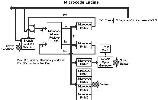
The Q register contents may be modified by the microcode in the course of execution of an instruction, so references to Q by the microcode are not always to the 'proper' instruction encoding. A multi-way branch is performed by directing several bits of the Q register to become the primary-address modifier.
Two-way branches are implemented by selecting 1 of 16 1-bit conditions, the state of the condition will affect the lowest bit of the microcode address (SM0). The ROM PM bits do double-duty as the branch condition selector, consequentially when a branch decision is specified (BRC), the next primary-address bits are fixed to the XOR combination of the current address and the branch condition selection. With this constraint on specifying the next address, the microcode program tends to jump all over the ROM address space.
A flowchart of the microcode is presented in the patent. The ROM data contents were included in the patent and have been used to produce a disassembly of the microcode. The following tables are a summary of the micro-operation fields and encoding:
| Microcode Operation Fields & Encoding | |||
|---|---|---|---|
| |||
| |||
| |||
Instructions require multiple micro-operations, the number varying with the type of instruction.
The implementation appears to have prioritised hardware minimisation over speed, even simple instructions tend to require quite a few microcode operations.
The ADA/B instruction (add memory to register), for example, involves 12 micro-operations.
Below is the typical sequence for the ADA/B instruction:
| Example Micro-operation Sequence: ADA/B Instruction |
|---|
Address    Next Address   Shifting Special           Dataflow -->               Description
--------  --------------  --------  ---  ----------------------------------- ---------------------------------------------------------------------
                Br  Fail  SCK  Sh
Dec PASA  PASA Cond PASA  Cyc Cond       XTR   RC    SC    AC    XC  TTM TTT
=== ====  ==== ==== ====  === ====  ===  === ======= === ======= === === === =====================================================================
234 1612  0616             12                RDM.ZTR ZTS ZTT.CBC NOP         load T with instruction from memory
110 0616  1213 QNR  1212   16                  UTR   TTS   AND   TTQ         transfer T to Q, also branch for interrupt

171 1213  0012 QMR  0013    1                  ZTR   ZTS   ZTT   QAB         select A/B, branch for memory-reference class

 10 0012  1313 Q10  1312   10                  ZTR   TTS   IOR   NOP TTM     load M with 10 LSBs of address from instr, branch for base/current page
187 1313  1102              6                  ZTR   MTS   ZTT   NOP         rotate M 6 more bits to form current-page address
146 1102  0003 Q15  0002   12                RDM.ZTR ZTS ZTT.CBC NOP         load T with operand from memory, branch for direct/indirect

  2    2  1700              1  QRD  QPM  XTR   UTR   ZTS   ZTT   NOP         multi-way branch on instruction type

  0    0  0005             16            XTR         TTS   ADD   TTX         Add: A/B + T -> A/B
  5 0005  0704  BC  0705    1   BC             ZTR   UTS   IOR   TBE         set E bit if binary carry set, and branch
116 0704  0202              3                  ZTR   ZTS ZTT.CBC TBE         clear 3 more bits of E if binary carry was set

 34 0202  1603              1                  PTR   UTS   ADD   TTP TTM     add 1 to P at LSB, load result into M
227 1603  1612             15                  PTR   ZTS   ADD   TTP TTM     ripple-carry through 15 bits of P, load M
                          ---
                           94
|
microcode cycle = (1 + (1..16)) * 125nS
                = 250 .. 2125 nS
                == 4MHz .. 471KHz
The ADA/B instruction listed previously takes 94 MCK cycles, with 12 more for the per-operation overhead:
ADA/B time = (94+12) MCK * 125nS/MCK
= 13.25 �S
This is the equivalent of a not-very-speedy 75,000 instructions per second. In comparison, on the HP 2116 an ADA/B instruction takes 3.2 �S == 312,000 IPS.
RAM memory refresh further reduces the effective instruction rate. As explained further below, the processor is halted for 20 out of every 840 �S for refresh, reducing the processing rate by 2.4%.
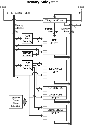 The architecture provides for a 32 KW address space.
The lower 16KW is reserved for the firmware ROMs.
Varying amounts of RAM were in the upper 16KW.
The architecture provides for a 32 KW address space.
The lower 16KW is reserved for the firmware ROMs.
Varying amounts of RAM were in the upper 16KW.
7.5 KW of ROM are standard/required for the firmware, split between between the BASIC ROM board (7KW in 28 chips) and the BASIC II ROM board (512W in 2 chips, 512W of unused address space). The other 8KW space addresses the option ROMs (3 slots, 1KW each) and cartridge ROMs (5 slots, 1KW each).
The original set was followed by the "standard" set, which had both 4KW boards and 2KW boards, but also new M-Register and T-Register boards.
Both the original and standard set were implemented with the historic Intel 1103 1K*1 dynamic RAM chip, the first RAM IC to start putting a dent in the hegemony of core memory. The 4KW boards were densely packed with 64 1103 chips.
There are slots in the backplane for only two memory boards, so the machine was limited to 4KW with the original set and 8KW with the standard set. Note that the architecture allows for a maximum of 16KW RAM. Some comments in the patent and extra signals on the external I/O slots suggest there may have been the intention to provide for expanding RAM memory in an external case. The extra signals - which were not needed by general I/O interfaces - were used by the disk I/O sub-system.
The 9830A was superseded in 1976 by the 9830B, the primary difference being the ability to increase the RAM from 8KW to a full 16KW. This was accomplished with a third RAM board-set, with 8KW per memory board using TMS4060 4K-bit chips. Once again, a new M-Register board was also required.
| HP9830 RAM Board-Sets | |||||||
| Board-Set | M-Register Board | T-Register Board | Memory Board | Chip | Chip Size | Words / Board | Max. RAM Memory |
|---|---|---|---|---|---|---|---|
| 09830-69522 | 09830-69523 | 09830-69524 | 1103 | 1K * 1 | 2 KW | 4 KW | |
| 09830-66582 | 09830-66583 | 09830-66584 | 1103 | 1K * 1 | 2 KW | 4 KW | |
| " | " | 11275-66584 | 1103 | 1K * 1 | 4 KW | 8 KW | |
| 9830B | 09830-66592 | " | 09830-66594 | TMS4060 | 4K * 1 | 8 KW | 16 KW |
The "standard" board-set was the most prevalent and the remainder of information on this site is derived from and focussed on this set.
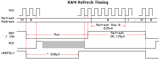
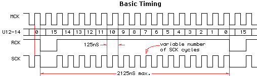
Refreshing of the dynamic RAM chips is accomplished by simply halting the processor periodically and executing a sequence of memory access cycles while halted. In each refresh period, 32 memory access cycles are performed, one for each row in the 1103 chips. The refresh memory access cycles each require 5 MCK cycles. An additional MCK cycle is needed to transition into the refresh period, thus:
refresh period = (32*5 + 1) * 125nS
= 20.125 �S
The run period is determined by the refresh delay monostable, and so varies with RC tolerances. The calculated design target for the monostable is 820 �S (based on the RC values on one instance of the M board). The start of refresh has to wait for the end of the current microcode cycle, so the run period may be up to ~ 2�S longer. Each refresh cycle only refreshes half the RAM memory banks, with a given bank being refreshed on alternate cycles. The refresh rate is approximately:
refresh rate = 2 * (820+2+20)�S
= 1684 �S
== 594 Hz
The 1103 datasheets specify a minimum refresh rate of 500Hz (2mS).
The access cycles for the 1103s are complex enough that a small 4-bit state machine is used to sequence the control signals for the 1103s. The memory cycle state machine implements 3 types of cycle: read, write and refresh. Some analysis and a spreadsheet simulation of the state machine logic indicates a read-cycle takes 10 MCK cycles, a write-cycle takes 11, and - as mentioned above - a refresh-cycle takes 5. The microcode flowchart indicates 10-bit microcode cycles for both read and write, while the patent microcode ROM data specifies 12-bit cycles for both read and write.
The same state machine and read-cycle are used for reading from the ROMs even though the accessing requirements are much simpler. It would be interesting to know what the speed specifications for the HP ROM chips actually was, in that if it was significantly faster than the > 1 µS cycle time of the state machine, it should have been possible to implement a 4th and faster cycle for ROM reads.
For such reasons, a small amount of RAM and ROM are swapped so there will be some RAM within the zero-page (lowest 1KW), for use by the system.
Some unfortunate logic in the address decoding swaps 256 bytes of ROM at the top quarter of the zero-page (001400-001777) with the first 256 bytes of RAM (040000-040377).
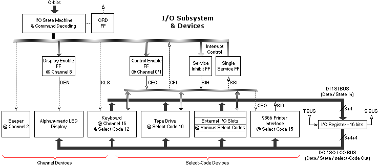 The 2116 architecture set out a fairly straightforward and consistent I/O architecture, with a 16-bit I/O bus and each device having a control-bit and a flag-bit (more detail).
There were 9 I/O instructions and devices were addressed by a channel number embedded in I/O instructions.
The 2116 architecture set out a fairly straightforward and consistent I/O architecture, with a 16-bit I/O bus and each device having a control-bit and a flag-bit (more detail).
There were 9 I/O instructions and devices were addressed by a channel number embedded in I/O instructions.
At the machine-instruction level, this scheme has been retained in the 9830, but another level of complexity has been added.
A select-code device is addressed by specifying the select-code in the upper 4 bits of a word output to channel 1. Usage of the other 12 output bits is determined by the specific device but general policy is the lowest 8 bits are a byte of data and the remaining 4 bits a command/state directive. A similar policy applies for input words, the lowest 8 bits are data, the next 4 are device state information. The uppermost 4 are not used on input.
I/O operations and devices are covered in further depth on the Machine Architecture page.
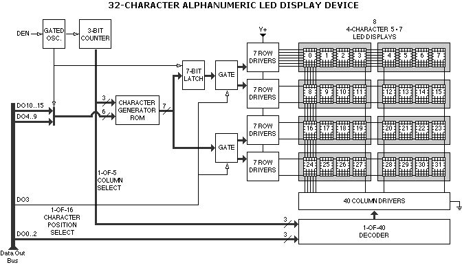 The 32-character display is made up from eight 4-character 5*7 dot-matrix LED displays.
These were made (and sold) by HP.
The 32-character display is made up from eight 4-character 5*7 dot-matrix LED displays.
These were made (and sold) by HP.
For multiplexing, the display is broken into 2 groups of 16 (lower and upper halves of the display line) and the two groups scanned in parallel, column by column. For example, character positions 3 and 19 are scanned at the same time, and at a given instant there may be up to 14 LEDs being illuminated. The duty cycle per LED or column is then ~ 1/80=1/(16*5). The on-time for a column is 88µS, determined by two monostables forming a gated oscillator. A digit is scanned in 440µS, and the full display in ~ 7mS.
The LEDs are physically organised into a 28-row * 40-column matrix, not 14*80 as might be anticipated (or 7*160).
A total of 68 drivers are then required, which is as close as could be expected to the 2D minimum of
The display hardware takes care of generating the 7-row pixel patterns with a Texas Instruments MOS character-generator ROM, and of scanning the 5 columns within each character. The firmware is still involved in the multiplexing however. The firmware must periodically deliver two 6-bit ASCII character codes to the device along with a 4-bit address to select the character positions, via the I/O Data Output bus (DOx), and trigger the display-enable (DEN) signal. DEN enables the gated oscillator for the 5-column scan of the two character positions. The oscillator multiplexes the character ROM between the two character groups - note the 7-bit latch for one group at the output of the ROM. The other group relies on stable data on the DO bus through the ROM during the scanning interval.
The gated oscillator is formed by the two monostables of IC U42-c3, the other two monostables in the circuit (U42-c2) are not strictly necessary functionally, they appear to be present to protect the LEDs in the event of failure in the firmware scanning. In particular, the scanning could be upset by a problem on the DO bus which is externally accessible via the I/O slots.
The design and the ROM character generator work on the opposite scanning orientation to the character generators typically used for raster-scan video terminals. The ROM is from the TMS4100 series of character generators produced by TI, but (as Rob pointed out) the lazy-T prompt character of the 9830 is not a standard character, so the ROM was not an off-the-shelf IC.
At the machine level, the display device is located at I/O channel 8.
An "OTA/B 8" instruction sends the ASCII codes and character position to the device and sets the DEN flag.
A "CLF 8" instruction clears the DEN flag.
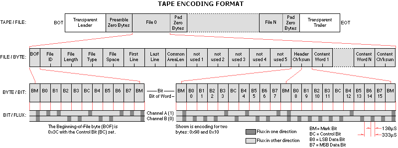
Two channels on tape are used to encode a single bit stream. A flux pulse in one channel indicates a zero in the bit stream, a flux pulse in the other channel indicates a one. This scheme makes clock extraction trivial and is tolerant of wide speed variation.
Flux pulses occurring simultaneously in both channels are a mark and are used as a byte delimiter. There are nine content bits in a byte: 8 data bits and a control bit. With the mark bit there are an average of 10 bits/byte. When writing, a mark is written at the beginning of the first byte and at the end of every byte, so there is a mark at the beginning and end of every byte, but only one mark between bytes. When reading, bytes must be fully formed - 9 bits between marks - to be recognised by the drive as a valid byte. This avoids delivery of incomplete bytes when reading begins in the middle of a byte, or bytes which were malformed by partial overwrite when a portion of a tape is rewritten.
The control bit is used to indicate a control - or interrupting - byte. Only one control byte is defined: the Beginning-of-File byte (control-0x3C). When finding a file, the drive is set to read in control mode, and (only) BOF bytes are recognised by the drive, and generate an interrupt to the processor. Note also that 0x3C, with the control bit in the middle, has a symmetric bit order, so the same hardware will detect the BOF byte when reading in reverse as well as forward.
When writing, head current in both channels is turned on at the beginning of the write. The bit period is determined by two monostables - one of ~ 200 �S and one of ~ 130 �S - configured as a loopback oscillator. To produce a flux pulse, the current in a channel head is reversed for the 130 �S interval. As current is always flowing in the head in one direction or other during writing, any prior data on the tape is erased. The basic bit and byte rates are:
bit rate = 200�S + 130�S
= 330 �S/bit
== 3000 bits/S
byte rate = 330 �S/bit * (8+1+1) bits/byte
= 3.3 mS/byte
== 300 bytes/S
Anomaly: The drive may read in either control mode or data mode. In control mode, normal indication of data bytes is inhibited and only control bytes will be indicated at the interface. In contrast, in data mode all bytes are delivered to the interface but without the control bit. In data mode, there is no way to distinguish a control byte from a data byte.
Aside from the padding bytes and the BOF byte, all data on the tape is in terms of two-byte 16-bit words, with the low-order byte coming first. The header fields are:
FileID         = 0..n sequence number of file
FileLength     = number of content words in use by file, not including checksum
FileType       = file type
FileSpace      = number of words for content reserved on tape, i.e. maximum FileLength
FirstLine      = first line number of program
LastLine       = last line number of program
CommonAreaLen  = number of words of program common area
Checksum       = sum of preceding header or content words, modulo 2^16

FileType   = 0 : file not in use
             1 : Binary block
             2 : Data
             3 : BASIC program
             4 : Key macros
             5 : Special program file
            21 : Secured binary block
            23 : Secured BASIC program
            24 : Secured key macros
            25 : Secured special program file
There is no explicit last file or end-of-files indicator.
Note that normal stereo audio cassette recording is 4-track and double-sided (2 sides, 2 tracks per side). Normal mono audio cassette recording is 2-track and double-sided (2 sides, 1 track per side). As such, neither of the common cassette heads is compatible with the 9830/65 head.
By calculation from component values, the gain for the head amps is set in the range of 500 to 600. The output from the head amps is typically around 1.5 to 2V (observed), the output from the heads should thus be around 2.5 to 3mV.
The sensor relies on the cassette having a transparent leader for optical transmission and a sufficiently reflective case to reflect light from the lamp back to the LDR. If the cassette case is not sufficiently reflective, if the tape leader does not have sufficient transparency, or if the bulb burns out, the drive will not be able to detect the BOT/EOT and not know to stop the motor at end of tape or when rewinding.
The LDR sensors can also fail. One failure mode is the LDR becomes leaky and will not reach a high enough dark resistance to trip the comparator. In one instance, a faulty LDR would not go above ~ 14K when dark, which is too low for the comparator to recognise as dark. In such cases the drive will always think the tape is in leader, hence at the BOT or EOT. The drive will run when commanded but run at the 'slow' speed because it thinks it is in leader. Pressing the REWIND button will rewind tape very slowly while the button is held, but the drive will not latch into rewind.
In operation, the LDR sense level and comparator input can be observed at A65-TP1. When magnetic tape is over the sensor, TP1 should be less than 2.5V. For leader, TP1 should be greater than 2.5V. As measured in one unit with the original lamp/LDR pair: tape=0.1V, leader=4.5V. These imply resistances for the LDR of tape=900K, leader=2K.
It is possible to replace the incandescent lamp with an LED and the LDR with a phototransistor.
Anomaly: A transition into leader at either BOT or EOT will stop the drive. When tape movement is initiated when in leader, the drive begins at slow speed but must continue regardless of the direction specified as it cannot distinguish between BOT and EOT. So, for example, a rewind command when the tape is already rewound will result in the drive jamming on attempting to rewind the tape, and similarly for a forward command issued when at EOT.
In practice, ordinary audio cassettes can be used, as long as the leader is transparent. Non-reflective cases may be modified by painting the appropriate surface in the cassette white or sticking a piece of white paper at the back of the compartment.
The actual magnetic tape does not seem to be critical. The recording method is a fairly simple and low density saturation recording. Cheap audio cassettes and CrO2 types have been successfully tried.
Pressure Pad Problems: Cassettes have an integral pressure pad behind the tape to hold the tape in close contact with the head. Two forms of pressure pads have been observed: a piece of foam with felt pad, and a metal band spring with felt pad. This applies to both audio cassettes and the HP-marked ones.
In many cassettes with the foam pad the foam has deteriorated, resulting in poor signal levels and erratic read/write operations. The foam pressure pads can be rebuilt with some new foam and double-sided tape, or in some cases a band-spring pad may be scavenged from another cassette and used to replace the foam-type pad.
|
Gallery
| Machine
| Hardware
| Microcode
| ALU
| Memory Cycles
| Unit Log
HP 9830 |
bhilpert 2013 Oct |