| HP 9830 |
HP 9830
Machine Architecture |
|
 This page presents a summary of the machine-instruction level of the 9830 processor.
The 9830 CPU is based on the architecture of the earlier HP 2116 series, a 16-bit, two-accumulator design.
The programming model of the 2116 is largely applicable to the 9830 but there are significant changes from the 2116 instruction set.
A list of differences is presented further below.
This page presents a summary of the machine-instruction level of the 9830 processor.
The 9830 CPU is based on the architecture of the earlier HP 2116 series, a 16-bit, two-accumulator design.
The programming model of the 2116 is largely applicable to the 9830 but there are significant changes from the 2116 instruction set.
A list of differences is presented further below.
Instruction Set
The table of instruction encodings below is largely a reiteration of that presented in the patent, with some examination of the microcode to clarify some issues.
For more details, particularly of the MAC group BCD instructions, see the patent (UKP-pg101).
The instruction set is broadly divided into 5 groups:
Notes:
- All instructions occupy 1 word.
- In memory reference instructions, the 10 m bits will be qualified by the zero/current-page bit p to produce a 15-bit address.
That address may then be further replaced recursively as directed by the indirect bit i.
- In binary additions, E is set to 1 upon carry out of bit 15 (MSB). The addition only sets E, it does not clear it.
- "Skip" means skip the next instruction.
- Branch offsets bbbbb are signed calculations from the address of the branch instruction.
- For right-shift instructions, the shift count is nnnn+1.
For left-shift, the shift count is 16-nnnn.
- The patent specifies STx, ISZ, DSZ, and JSM instructions of the D/I group may only be used in indirect mode.
These instructions require a destination memory address.
The same restriction should be applied to the JMP instruction, in that it makes no sense to jump to the A or B register.
In the microcode, the M register is expected to contain the destination address by the time the multiway branch to distinguish the instructions is executed at PASA=0002.
In direct instructions of the D/I group, M still contains the instruction address at this point.
STx, ISZ, DSZ will write to the instruction address, JSM and JMP will loop to themselves, with JSM overflowng the stack.
- The alignment of fields in the instruction encoding table in the US patent is confusing in some locations,
such as the shift code in the Shift-Rotate group.
- In both US & UK patents, SES & SEC have A/B register-select bit specified when it is irrelevant. Presumed to be 0.
| Instruction Set |
|---|
| Key: |
r : A=0 / B=1 register                   m : bit of 10-bit memory address
g : A=0 / B=1 register                   b : bit of 5-bit branch offset
i : Direct=0 / Indirect=1 addressing     d : bit of 5-bit I/O device channel
p : Zero=0 / Current=1 page              n : bit of 4-bit shift count
s : Hold=0 / Set=1 applicable bit        . : not used
c : Hold=0 / Clear=1 applicable bit
|
|
Opcode    MSB Bit Encoding  LSB       Description
------    ---------------------       -------------------------------------------------------------------
|
Memory Reference Group:
|
ADr       i 000 rpm mmm mmm mmm       A/B+[m] --> A/B, if carry 15: 1 --> E     \ ADd to A/B

CPr       i 001 rpm mmm mmm mmm       Skip if A/B <> [m]                        \ ComPare to A/B

LDr       i 010 rpm mmm mmm mmm       (m) --> A/B                               \ Load A/B

STr       i 011 rpm mmm mmm mmm       A/B --> [m]                               \ Store A/B

IOR       i 100 0pm mmm mmm mmm       A OR [m] --> A                            \ Inclusive OR
ISZ       i 100 1pm mmm mmm mmm       [m]+1 --> [m], skip if [m] = 0            \ Increment, Skip if 0

AND       i 101 0pm mmm mmm mmm       A AND [M] --> A                           \ bitwise AND
DSZ       i 101 1pm mmm mmm mmm       [m]-1 --> [m], skip if [m] = 0            \ Decrement, Skip if 0

JSM       i 110 0pm mmm mmm mmm       P-->[SP], SP+1-->SP,  m-->P               \ Jump to SuBroutine
JMP       i 110 1pm mmm mmm mmm       m --> P                                   \ Jump
|
D/I Reference Group:
|
ADr g     0 111 g.. i00 0r1 111       A/B(r)+A/B(g) --> A/B(r), if carry 15: 1 --> E

CPr g     0 111 g.. i00 1r1 111       Skip if A/B(r) <> A/B(g)

LDr g     0 111 g.. i01 0r1 111       A/B(g) --> A/B(r)

STr g     0 111 g.. 101 1r1 111       A/B(r) --> [A/B(g)]                       \ indirect only

IOR g     0 111 g.. i10 001 111       A  OR A/B(g) --> A
ISZ g     0 111 g.. 110 011 111       [A/B(g)]+1 --> [A/B(g)], skip if A/B = 0  \ indirect only

AND g     0 111 g.. i10 101 111       A AND A/B(g) --> A
DSZ g     0 111 g.. 110 111 111       [A/B(g)]-1 --> [A/B(g)], skip if A/B = 0  \ indirect only

JSM g     0 111 g.. 111 001 111       P-->[SP], SP+1-->SP,  A/B(g)-->P          \ indirect only
JMP g     0 111 g.. i11 011 111       A/B(g) --> P

EXr       0 111 r.. ... 001 110       Execute A/B as instruction
DMA       0 111 0.. ... 011 110       DMA
CMr       0 111 r.. ... 101 110       One's Complement A/B
TCr       0 111 r.. ... 111 110       Two's Complement A/B
|
Shift-Rotate Group:
|
ArR       0 111 r.. nnn n.0 000       Arithmetic Shift A/B Right
SrR       0 111 r.. nnn n.0 010       Shift A/B Right, 0 --> sign,MSBs
SrL       0 111 r.. nnn n.0 100       Shift A/B Left, 0 --> LSBs
RrR       0 111 r.. nnn n.0 110       Rotate A/B Right
|
Alter-Skip Group:
|
SZr       0 111 r0b bbb b01 000       Branch if A/B = 0
RZr       0 111 r1b bbb b01 000       Branch if A/B <> 0

SIr       0 111 r0b bbb b11 000       Branch if A/B = 0,  A/B+1 --> A/B
RIr       0 111 r1b bbb b11 000       Branch if A/B <> 0, A/B+1 --> A/B

SLr       0 111 rsb bbb bc1 001       Branch if A/B LSB = 0,         hold/clear/set --> LSB
SrM       0 111 rsb bbb bc1 010       Branch if A/B <  0 (bit 15=1), hold/clear/set --> bit 15
SrP       0 111 rsb bbb bc1 011       Branch if A/B >= 0 (bit 15=0), hold/clear/set --> bit 15

SES       0 111 0sb bbb bc1 100       Branch if E LSB = 1, hold/clear/set --> E (all 4 bits)
SEC       0 111 0sb bbb bc1 101       Branch if E LSB = 0, hold/clear/set --> E (all 4 bits)
|
Input/Output Group:
|
STF       1 111 .10 111 1dd ddd       1 --> device flag
CLF       1 111 .11 111 1dd ddd       0 --> device flag
SFC       1 111 .1c 111 0dd ddd       Skip if device flag = 0 (busy),  hold/clear flag
SFS       1 111 .1c 101 0dd ddd       Skip if device flag = 1 (ready), hold/clear flag

CLC       1 111 .1c 101 1dd ddd       0 --> device control bit, hold/clear flag
STC       1 111 .1c 110 0dd ddd       1 --> device control bit, hold/clear flag

OTr       1 111 r1c 001 1dd ddd       A/B --> device buffer,        hold/clear flag  \ OuTput A/B
LIr       1 111 r1c 010 1dd ddd       device buffer --> A/B,        hold/clear flag  \ Load Into A/B
MIr       1 111 r1c 000 1dd ddd       device buffer OR A/B --> A/B, hold/clear flag  \ Merge Into A/B
|
MAC Group:
|
RET       1 111 000 100 000 010       SP-1 --> SP, [SP]+1 --> P                 \ return from subroutine

MOV       1 111 000 000 000 010       E-->A0..3, 0-->A4..15, 0-->E
CLR       1 111 000 000 000 000       clear 4 words [A+0..3]
XFR       1 111 000 000 000 100       transfer 4 words [A+0..3] --> [B+0..3]
MRX       1 111 100 100 011 000       shift mantissa right AR1
MRY       1 111 100 100 111 000       shift mantissa right AR2
MLS       1 111 001 100 000 000       shift mantissa left AR2
DRS       1 111 000 100 001 000       shift mantissa right AR1
DLS       1 111 101 100 000 000       shift mantissa left AR1
FXA       1 111 000 101 110 000       fixed point addition
FMP       1 111 001 100 110 000       fast multiply
FDV       1 111 000 100 010 000       fast divide
CMX       1 111 100 100 000 000       10's complement AR1
CMY       1 111 000 100 000 000       10's complement AR2
MDI       1 111 000 101 100 000       mantissa decimal increment
NRM       1 111 001 100 101 000       normalise
|
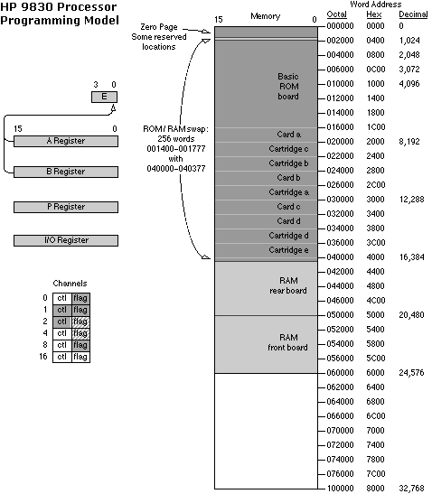
Reserved Memory Locations
| Reserved Memory Locations |
| Address | Use |
|---|
| 00000 | Reset instruction, the instruction at this location is executed upon Reset (POP). |
| 00001 | Constant used by microcode (counter in BCD instructions). |
| 00002 | Interrupt instruction, the instruction at this location is executed upon Interrupt (service request). |
| |
| 01700 | Temporary used by microcode (P storage during BCD instructions). |
| |
| 01744 | AR1 exponent & mantissa sign |
| 01745 | AR1 mantissa D0..3 |
| 01746 | AR1 mantissa D4..7 |
| 01747 | AR1 mantissa D8..11 |
| |
| 01754 | AR2 exponent & mantissa sign |
| 01755 | AR2 mantissa D0..3 |
| 01756 | AR2 mantissa D4..7 |
| 01757 | AR2 mantissa D8..11 |
| |
| 01777 | Stack pointer. Used by the JSM and RET instructions for subroutine return addresses. |
A few memory locations are treated specially by the processor microcode, listed in the table to the right.
The stack pointer points to the top of a stack area in RAM (next available location) for subroutine return addresses.
The stack grows up as subroutines are invoked.
AR1 and AR2 are 4-word floating-point BCD arithmetic registers referenced by instructions of the MAC group.
D0..11 are BCD digits of the mantissa, D0=MSD, D11=LSD.
The exponent is an 8-bit signed binary located in the upper byte of the first word.
The mantissa sign is the LSB of the first word.
Interrupts
When an interrupt occurs the contents of memory location 2 are executed as an instruction without first loading the program counter (P).
Instead, P is decremented by 1.
Consequently, if the instruction at location 2 is a JSM to an interrupt service routine, the return address placed on the stack will be the address just ahead of the instruction about to be executed when the interrupt occurred.
The RET instruction increments the return address it pops off the stack, so when the interrupt service routine executes a RET it will return to the desired restart address.
An interrupt sets the service-inhibit flag (SIH) so the interrupt servicing will not be re-interrupted.
An interrupt service subroutine will typically clear the flag upon exit.
I/O Channel Operations
There are only 6 channels used on the 9830, with dedicated applications, fixed in the hardware.
Channels 2 & 4 are used for the magnetic card reader and internal printer on the 9810/20 calculators and are not used on the 9830, except for the BEEP trigger on channel 2.
While the channel / control-bit / flag-bit I/O paradigm of the 2116 is formally retained in the instructions, in practice it is contorted a fair bit for the particular needs of various devices.
For example, the CLF instruction clears the DEN (display enable) flag, but STF does not set it, instead it is set by the OTA instruction - and it would make more sense in terms of the paradigm if the DEN flag were the control bit instead of the flag bit.
|
I/O Channel Operations
|
| Channel |
Use |
CLC |
STC |
CLF |
STF |
SFC |
SFS |
OTr |
LIr |
MIr |
| 0 |
Select-code devices |
- |
- |
- |
- |
Skip if
not STOP key |
Skip if
STOP key |
A/B7..0 -> IOR7..0
rotate A/B 8 bits
nCEO=0 |
IOR7..0 -> A/B15..8
nCEO=0 |
IOR7..0 OR'd -> A/B7..0
rotate A/B 8 bits
nCEO=0 |
| 1 |
Select-code devices |
- |
nCEO=0 |
nSIH=1
IOR.SC=0
nCEO=1 |
nSIH=0
DI bus -> IOR
nCEO=1 |
Skip if
nCEO=0 |
Skip if
nCEO=1 |
A/B -> IOR |
IOR -> A/B |
IOR OR'd -> A/B |
| 2 |
9810/20:
Magnetic-card reader |
- |
MLS=+pulse
9830: BEEP |
MCR FF=0 |
MCR=+pulse |
Skip if
MCR FF=0 |
Skip if
MCR FF=1 |
- |
- |
- |
| 4 |
9810/20:
Internal printer
| - |
- |
PEN FF=0 |
- |
Skip if
PEN FF=0 |
Skip if
PEN FF=1 |
A/B -> IOR
PEN FF=1 |
- |
- |
| 8 |
Display |
- |
- |
nDEN FF=1 |
- |
ns |
ns |
A/B -> IOR
nDEN FF=0 |
- |
- |
| 16 |
Keyboard |
- |
- |
KLS=+pulse |
- |
ns |
ns |
A/B -> IOR
KLS=+pulse |
- |
- |
Certain actions by devices on the I/O bus affect the I/O Register (IOR) and flags:
- On interrupt (nSSI=0): DI bus -> IOR, nCEO=1 : capture device ID. ID is indicated by device asserting an identifying bit on the DI bus to low.
- On device ready (nCFI=0): DI bus -> IOR, nCEO=1 : capture data when device indicates ready by asserting CFI.
Note the IOR is a single 16-bit register used for both input and output. Output operations load the IOR from A or B, with the result appearing immediately on the output bus lines.
Input operations however, load A or B from the IOR, not directly from the input bus.
A load of the IOR from the input bus must be ensured to obtain newly-input data.
I/O Select-Code Devices
As mentioned on the hardware page, channels 0 and 1 are used for the Select-Code devices - those devices which are accessed by a select-code at the user level (e.g. LOAD BIN #9),
as well as the printer (SC #15) and internal tape drive (SC #10).
For Select-Code devices the input and output bus signals are distinguished into several groups.
The 16 output-bus signals become:
- DO12-15 = CO0-3: 4 select-code bits. Device interfaces decode these bits to determine whether the device is being addressed.
- DO8-11 = SO0-3: 4 command bits.
- DO0-7 = DO0-7: 8 data output bits.
12 of the 16 input-bus signals become:
- DI8-11 = SI0-3: 4 status bits.
- DI0-7 = DI0-7: 8 data input bits.
Input operations on the I/O Register do not load the high 4 bits of the IOR so as not to disrupt the select-code and hence device-selection.
The input and output operations on channel 0 are designed to support byte packing into, and unpacking out of, double-byte words.
CEO is the Control-Enable-Output.
In conjunction with the device-selection bits CO0-3, assertion of CEO initiates an I/O operation on a device.
Through the CFI (Channel-Flag-Input), CEO also may function as an acknowledge/ready indication back to the processor.
Select-Code devices may be distinguished as operating in General-Mode or Fast-Mode, as discussed next.
GENERAL-MODE:
These devices support simple stream input and output.
One command bit and one status bit are assigned dedicated purposes:
- Command bit SO3/DO11 is the transfer direction bit: 0=output operation, 1=input operation.
- Status bit SI0/DI8 is the ACK/RDY bit: 0=device busy, 1=device ready / operation complete.
The device interface is responsible for implementing a flag FF to hold state for this signal.
General-Mode devices pulse CEO to initiate an operation but do not leave it asserted.
The normal sequence of an operation is:
- If output op, processor puts select code on CO0-3, data on DO0-DO7, and sets SO3=0, via IOR.
- If input op, processor puts select code on CO0-3, and sets SO3=1, via IOR.
- Processor pulses nCEO=0 to initiate the operation, this pulse sets SI0=0.
- Processor polls SI0. It must load SI0->IOR->A/B to do so.
- If input, device puts data on DI0-DI7.
- The device sets SI0=1 when the operation is complete, the processor detects this in poll.
- If input, processor gets data from DI0-7 via IOR0-7.
The 9866 printer and interfaces such as the TTL interface (11202A) use General-Mode.
The firmware assumes the protocol for General-Mode devices in such routines as PRINT, WRITE, PTAPE, etc.
FAST-MODE:
These devices assert CEO to initiate an operation and leave it asserted.
The device uses the CFI line to deassert CEO, this functions as ack for the operation.
Command bit and status bit usage is device specific.
The normal sequence of an operation is:
- Processor puts select code on CO0-3, data if applicable on DO0-DO7, and command on SO0-SO3.
- Processor sets nCEO=0 to initiate the operation.
- Processor polls CEO.
- If input op, device puts data on DI0-DI7 and status on SI0-SI3.
- The device sets nCFI=0 when the operation is complete. This deasserts CEO (nCEO=1), which the processor detects in poll.
- Processor gets status & data from SI0-3 & DI0-7 via IOR.
The cassette tape drive(s) operate in Fast-Mode.
Differences Between the 9830 and 2116 Machine Levels
Some of the differences between the 9830 and 2116 at the machine-instruction level:
- The machines are not machine-code compatible.
The instruction encoding, while similar in rough format, is in detail thoroughly different.
- The 2116 used 'skip-next-instruction' style conditional branching.
The 9830 implements most of the conditional branches as actual branch instructions with a 5-bit signed offset (+15/-16), even though still calling them skips.
- The 'micro-instruction' ability of the 2116 to combine certain instructions into one instruction word is gone.
In some cases this loss is compensated for by the addition of functionally equivalent instructions, such as TCx (twos-complement of A/B) replacing the CMx,INx sequence, and added facilities in the Alter-Skip Group instructions to set and clear various bits.
- The XOR instruction is gone, replaced by the DSZ (decrement, skip if zero) instruction.
- BCD arithmetic instructions have been added.
- There are a few other new instructions: EXA/B, DMA.
- Use of the addresses 0 & 1 as synonyms for the A & B registers is gone.
The functionality is largely replaced by the D/I Group instructions.
- The E register is now 4 bits, instead of 1.
- The overflow flag for binary addition is gone.
- In the 2116 the first word of a subroutine was used to hold the return address, which doesn't work very well with ROM.
In the 9830, the return address for subroutines has been moved to a stack in RAM.
- The I/O channel number encoding is 5 bits instead of 6.
- A second device-interfacing scheme is added to the channel scheme.
- The interrupt facility is simplified to a single interrupt.
There is no hardware prioritising or vectoring for interrupts.